- 您现在的位置:买卖IC网 > Datasheet目录466 > KAC-9617 (Eastman Kodak Company)IC SENSOR IMAGE VGA 48CLCC Datasheet资料下载
参数资料
| 型号: | KAC-9617 |
| 厂商: | Eastman Kodak Company |
| 文件页数: | 23/41页 |
| 文件大小: | 0K |
| 描述: | IC SENSOR IMAGE VGA 48CLCC |
| 标准包装: | 480 |
| 象素大小: | 7.5µm x 7.5µm |
| 有源象素阵列: | 648H x 488V |
| 每秒帧数: | 30 |
| 电源电压: | 3.3V |
| 类型: | CMOS 成像 |
| 封装/外壳: | 48-LCC |
| 供应商设备封装: | 48-LCC(14.22x14.22) |
| 包装: | 散装 |
| 请注意: | * |
| 其它名称: | LM9617 |
第1页第2页第3页第4页第5页第6页第7页第8页第9页第10页第11页第12页第13页第14页第15页第16页第17页第18页第19页第20页第21页第22页当前第23页第24页第25页第26页第27页第28页第29页第30页第31页第32页第33页第34页第35页第36页第37页第38页第39页第40页第41页
�� �
�
�IMAGE� SENSOR� SOLUTIONS�
�Functional� Description� (continued)�
�,�
�pclk�
�d[11:0]�
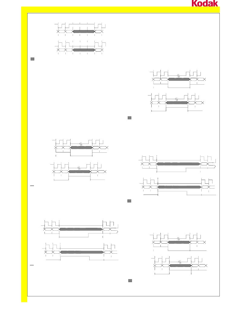
�11.4� Vertical/Horizontal� Synchronisation� Pin� (vsync)�
�The� vertical� synchronisation� output� pin,� vsync,� is� used� as� an�
�indicator� for� pixel� data� within� a� frame.� The� vsync� output� pin� can�
�a)� pclk� active� edge� negative�
�pclk�
�d[11:0]�
�b)� pclk� active� edge� positive�
�invalid� pixel� data�
�Figure� 38.� pclk� in� Data� Ready� Mode�
�By� default� the� pixel� clock� is� a� free� running� active� low� (pixel� data�
�changes� on� the� positive� edge� of� the� clock)� with� a� period� equal� to�
�be� programmed� to� operate� in� two� modes� as� follows:�
�?� Level� mode� should� be� used� when� the� pixel� clock,� pclk,� is� pro-�
�grammed� to� operate� in� free� running� mode.� In� level� mode� the�
�vsync� output� pin� will� go� to� the� specified� level� (high� or� low)� at�
�the� start� of� each� frame� and� remain� at� that� level� until� the� last�
�pixel� of� that� row� in� the� frame� is� placed� on� d[11:0]� as� shown� in�
�Figure� 41.� The� hsync� level� is� always� synchronized� to� the�
�active� edge� of� pclk� .�
�pclk�
�the� internal� hclk� .� The� active� edge� of� the� clock� can� be� pro-�
�grammed� such� that� pixel� data� changes� on� the� positive� or� nega-�
�tive� edge� of� the� clock.�
�d[11:0]�
�vsync�
�Frame� n�
�Frame� n+1�
�Frame� n+1�
�Frame� n�
�11.3� Horizontal� Synchronisation� Output� Pin� (hsync)�
�The� horizontal� synchronisation� output� pin,� hsync� ,� is� used� as� an�
�indicator� for� row� data.� The� hsync� output� pin� can� be� programmed�
�to� operate� in� two� modes� as� follows:�
�?� Level� mode� should� be� used� when� the� pixel� clock,� pclk,� is� pro-�
�grammed� to� operate� in� free� running� mode.� In� level� mode� the�
�hsync� output� pin� will� go� to� the� specified� level� (high� or� low)� at�
�the� start� of� each� row� and� remain� at� that� level� until� the� last�
�pixel� of� that� row� is� read� out� on� d[11:0]� as� shown� in� Figure� 39.�
�The� hsync� level� is� always� synchronized� to� the� active� edge� of�
�pclk� .�
�pclk�
�d[11:0]�
�a)� vsync� programmed� to� be� active� high�
�pclk�
�d[11:0]�
�vsync�
�b)� vsync� programmed� to� be� active� low�
�invalid� pixel� data�
�Figure� 41.� vsync� in� Level� Mode�
�?� Pulse� mode� should� be� used� when� the� pixel� clock,� pclk,� is� pro-�
�grammed� to� operate� in� data� ready� mode.� In� pulse� mode� the�
�vsync� output� pin� will� produce� a� pulse� at� the� end� of� each�
�frame.� The� width� of� the� pulse� will� be� a� minimum� of� four� hclk�
�cycles� and� its� polarity� can� be� programmed� as� shown� in� Figure�
�42.� The� vsync� level� is� always� synchronized� to� the� active� edge�
�hsyn� c�
�Row� n�
�Row� n+1�
�of� pclk� .�
�a)� hsync� programmed� to� be� active� high� (default)�
�pclk�
�pclk�
�d[11:0]�
�Row� n+1�
�Row� n�
�d[11:0� ]�
�hsync�
�b)� hsync� programmed� to� be� active� low�
�Figure� 39.� hsync� in� Level� Mode�
�vsync�
�pclk�
�d[11:0]�
�Frame� n� Frame� n+1�
�a)� vsync� programmed� to� be� active� high�
�?� Pulse� mode� should� be� used� when� the� pixel� clock,� pclk,� is� pro-�
�vsync�
�Frame� n�
�Frame� n+�
�grammed� to� operate� in� data� ready� mode.� In� pulse� mode� the�
�hsync� output� pin� will� produce� a� pulse� at� the� end� of� each� row.�
�The� width� of� the� pulse� will� be� a� minimum� of� four� pclk� cycles�
�and� its� polarity� can� be� programmed� as� shown� in� Figure� 40.�
�The� hsync� level� is� always� synchronized� to� the� active� edge� of�
�pclk�
�pclk�
�d[11:0� ]�
�b)� vsync� programmed� to� be� active� low� (default)�
�invalid� pixel� data�
�Figure� 42.� vsync� in� pulse� mode�
�11.5� Odd/Even� Mode�
�In� odd/even� mode� the� vsync� signal� is� used� to� indicate� when�
�pixel� data� from� an� odd� and� even� field� is� being� placed� on� the� dig-�
�ital� video� bus� d[11:0]� .� The� polarity� of� vsync� can� still� be� pro-�
�grammed� in� this� mode� as� shown� in� Figure� 43�
�hsync�
�Row� n�
�Row� n+1�
�pclk�
�Even� Field�
�Odd� Field�
�pclk�
�d[11:0]�
�a)� hsync� programmed� to� be� active� high�
�d[11:0]�
�vsync�
�a)� vsync� programmed� to� be� active� high� (default)�
�hsync�
�Row� n� Row� n+1�
�b)� hsync� programmed� to� be� active� low�
�Figure� 40.� hsync� in� Pulse� Mode�
�pclk�
�d[11:0]�
�By� default� the� first� pixel� data� at� the� beginning� of� each� row� is�
�vsync�
�Odd� Field�
�Even� Field�
�placed� on� the� digital� video� bus� as� soon� as� hsync� is� activated.� It�
�is� possible� to� program� up� to� 15� dummy� pixels� to� be� readout� at�
�the� beginning� of� each� row� before� the� real� pixel� data� is� readout.�
�This� feature� is� supported� for� both� level� and� pulse� mode.�
�b)� vsync� programmed� to� be� active� low�
�invalid� pixel� data�
�Figure� 43.� vsync� in� odd/even� Mode�
�www.kodak.com/go/imagers� 585-722-4385�
�23�
�Email:imagers@kodak.com�
�相关PDF资料 |
PDF描述 |
|---|---|
| KAC-9627 | IC SENSOR IMAGE VGA 48CLCC |
| KB-A100SRW | LIGHT BAR 660NM RED 8.89X3.81MM |
| KB-B100SRW | LIGHT BAR 660NM RED 19.05X3.81MM |
| KB-C100SRW | LIGHT BAR 660NM RED 8.89X8.89MM |
| KB-D100SRW | LIGHT BAR 660NM RED 8.89X3.81MM |
相关代理商/技术参数 |
参数描述 |
|---|---|
| KAC-9618 | 功能描述:IC SENSOR IMAGE VGA MONO 48-CLCC RoHS:是 类别:传感器,转换器 >> 图像,相机 系列:- 标准包装:480 系列:- 象素大小:6.7µm x 6.7µm 有源象素阵列:768H x 488V 每秒帧数:52 电源电压:3.3V 类型:CMOS 成像 封装/外壳:48-QFP 供应商设备封装:48-QFP 包装:托盘 请注意:* 配用:4H2105-ND - HEADBOARD FOR KAC-004014H2104-ND - KIT EVAL FOR KAC-00401 其它名称:4H20954H2095-NDKAC-00401-CBC-LB-A0 |
| KAC-9618/HEADBOARD | 功能描述:HEADBOARD FOR KAC-9618 RoHS:是 类别:编程器,开发系统 >> 过时/停产零件编号 系列:- 标准包装:1 系列:- 传感器类型:CMOS 成像,彩色(RGB) 传感范围:WVGA 接口:I²C 灵敏度:60 fps 电源电压:5.7 V ~ 6.3 V 嵌入式:否 已供物品:成像器板 已用 IC / 零件:KAC-00401 相关产品:4H2099-ND - SENSOR IMAGE WVGA COLOR 48-PQFP4H2094-ND - SENSOR IMAGE WVGA MONO 48-PQFP |
| KAC-9618EVAL-KIT | 功能描述:KIT EVALUATION SENSOR KAC-9618 RoHS:是 类别:编程器,开发系统 >> 过时/停产零件编号 系列:- 标准包装:1 系列:- 传感器类型:CMOS 成像,彩色(RGB) 传感范围:WVGA 接口:I²C 灵敏度:60 fps 电源电压:5.7 V ~ 6.3 V 嵌入式:否 已供物品:成像器板 已用 IC / 零件:KAC-00401 相关产品:4H2099-ND - SENSOR IMAGE WVGA COLOR 48-PQFP4H2094-ND - SENSOR IMAGE WVGA MONO 48-PQFP |
| KAC-9619 | 功能描述:IC SENSOR IMAGE VGA 48-CLCC RoHS:是 类别:传感器,转换器 >> 图像,相机 系列:- 标准包装:480 系列:- 象素大小:6.7µm x 6.7µm 有源象素阵列:768H x 488V 每秒帧数:52 电源电压:3.3V 类型:CMOS 成像 封装/外壳:48-QFP 供应商设备封装:48-QFP 包装:托盘 请注意:* 配用:4H2105-ND - HEADBOARD FOR KAC-004014H2104-ND - KIT EVAL FOR KAC-00401 其它名称:4H20954H2095-NDKAC-00401-CBC-LB-A0 |
| KAC-9619/HEADBOARD | 功能描述:HEADBOARD FOR KAC-9619 RoHS:是 类别:编程器,开发系统 >> 过时/停产零件编号 系列:- 标准包装:1 系列:- 传感器类型:CMOS 成像,彩色(RGB) 传感范围:WVGA 接口:I²C 灵敏度:60 fps 电源电压:5.7 V ~ 6.3 V 嵌入式:否 已供物品:成像器板 已用 IC / 零件:KAC-00401 相关产品:4H2099-ND - SENSOR IMAGE WVGA COLOR 48-PQFP4H2094-ND - SENSOR IMAGE WVGA MONO 48-PQFP |
发布紧急采购,3分钟左右您将得到回复。