参数资料
| 型号: | KAD2708C-27Q68 |
| 厂商: | Intersil |
| 文件页数: | 5/16页 |
| 文件大小: | 0K |
| 描述: | IC ADC 8BIT 275MSPS PAR 68-QFN |
| 产品培训模块: | High-Speed Analog-to-Digital Converters |
| 标准包装: | 1 |
| 系列: | FemtoCharge™ |
| 位数: | 8 |
| 采样率(每秒): | 275M |
| 数据接口: | 并联 |
| 转换器数目: | 1 |
| 功率耗散(最大): | 294mW |
| 电压电源: | 单电源 |
| 工作温度: | -40°C ~ 85°C |
| 安装类型: | 表面贴装 |
| 封装/外壳: | 68-VFQFN 裸露焊盘 |
| 供应商设备封装: | 68-QFN(10x10) |
| 包装: | 托盘 |
| 输入数目和类型: | 1 个差分,单极 |
13
FN6812.1
April 14, 2011
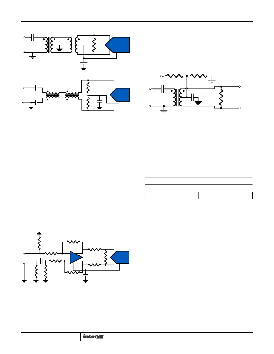
A back-to-back transformer scheme is used to improve
common-mode rejection, which keeps the common-mode
level of the input matched to VCM. The value of the
termination resistor should be determined based on the
desired impedance.
The sample and hold circuit design uses a switched
capacitor input stage, which creates current spikes when the
sampling capacitance is reconnected to the input voltage.
This creates a disturbance at the input which must settle
before the next sampling point. Lower source impedance will
result in faster settling and improved performance. Therefore
a 1:1 transformer and low shunt resistance are
recommended for optimal performance.
A differential amplifier can be used in applications that
require DC coupling, at the expense of reduced dynamic
performance. In this configuration the amplifier will typically
reduce the achievable SNR and distortion performance. A
typical differential amplifier configuration is shown in
Figure 25.
Clock Input
The clock input circuit is a differential pair (see Figure 29).
Driving these inputs with a high level (up to 1.8VPP on each
input) sine or square wave will provide the lowest jitter
performance. The recommended drive circuit is shown in
Figure 26. The clock can be driven single-ended, but this will
reduce the edge rate and may impact SNR performance.
Use of the clock divider is optional. The KAD2708C's ADC
requires a clock with 50% duty cycle for optimum
performance. If such a clock is not available, one option is to
generate twice the desired sampling rate, then use the
KAD2708C's divide-by-2 to generate a 50%-duty-cycle
clock. This frequency divider uses the rising edge of the
clock, so 50% clock duty cycle is assured. Table 2 describes
the CLKDIV connection.
CLKDIV is internally pulled low, so a pull-up resistor or logic
driver must be connected for undivided clock.
Jitter
In a sampled data system, clock jitter directly impacts the
achievable SNR performance. The theoretical relationship
between clock jitter and maximum SNR is shown in
Where tJ is the RMS uncertainty in the sampling instant.
This relationship shows the SNR that would be achieved if
clock jitter were the only non-ideal factor. In reality,
achievable SNR is limited by internal factors such as
differential nonlinearity, aperture jitter and thermal noise.
FIGURE 23. TRANSFORMER INPUT, GENERAL APPLICATION
ADT1-1WT
0.1F
KAD2708
VCM
50
O
0.01F
Analog
In
ADT1-1WT
Ω
ADTL1-12
0.1F
KAD2708
VCM
ADTL1-12
1nF
Analog
Input
25
O
25
O
FIGURE 24. TRANSFORMER INPUT, HIGH IF APPLICATION
Ω
KAD2708
VCM
0.1F
0.22F
69.8O
49.9O
100O
69.8O
348O
CM
151O
25O
+
Vin
-
FIGURE 25. DIFFERENTIAL AMPLIFIER INPUT
Ω
TABLE 2. CLKDIV PIN SETTINGS
CLKDIV PIN
DIVIDE RATIO
AVSS
2
AVDD
1
TC4-1W
1nF
AVDD2
200O
CLKP
CLKN
1kO
1nF
Clock
Input
FIGURE 26. RECOMMENDED CLOCK DRIVE
Ω
SNR
20 log10
1
2
πf
INtJ
--------------------
=
(EQ. 1)
KAD2708C
相关PDF资料 |
PDF描述 |
|---|---|
| KAD2708L-27Q68 | IC ADC 8BIT 275MSPS PAR 68-QFN |
| KAD2710C-27Q68 | IC ADC 10BIT 275MSPS PAR 68-QFN |
| KAD2710L-21Q68 | IC ADC 10BIT 210MSPS SGL 68-QFN |
| KAD5510P-25Q48 | IC ADC 10BIT CMOS 250MSPS 48QFN |
| KAD5510P-50Q72 | IC ADC 10BIT 500MSPS SGL 72-QFN |
相关代理商/技术参数 |
参数描述 |
|---|---|
| KAD2708L | 制造商:未知厂家 制造商全称:未知厂家 功能描述:8-Bit, 350MSPS Analog-to-Digital Converter |
| KAD2708L_11 | 制造商:INTERSIL 制造商全称:Intersil Corporation 功能描述:8-Bit, 350/275/210/170/105MSPS A/D Converter |
| KAD2708L-10Q68 | 功能描述:IC ADC 8BIT 105MSPS SGL 68-QFN RoHS:是 类别:集成电路 (IC) >> 数据采集 - 模数转换器 系列:FemtoCharge™ 产品培训模块:Lead (SnPb) Finish for COTS Obsolescence Mitigation Program 标准包装:250 系列:- 位数:12 采样率(每秒):1.8M 数据接口:并联 转换器数目:1 功率耗散(最大):1.82W 电压电源:模拟和数字 工作温度:-40°C ~ 85°C 安装类型:表面贴装 封装/外壳:48-LQFP 供应商设备封装:48-LQFP(7x7) 包装:管件 输入数目和类型:2 个单端,单极 |
| KAD2708L-17Q68 | 功能描述:IC ADC 8BIT 170MSPS SGL 68-QFN RoHS:是 类别:集成电路 (IC) >> 数据采集 - 模数转换器 系列:FemtoCharge™ 产品培训模块:Lead (SnPb) Finish for COTS Obsolescence Mitigation Program 标准包装:250 系列:- 位数:12 采样率(每秒):1.8M 数据接口:并联 转换器数目:1 功率耗散(最大):1.82W 电压电源:模拟和数字 工作温度:-40°C ~ 85°C 安装类型:表面贴装 封装/外壳:48-LQFP 供应商设备封装:48-LQFP(7x7) 包装:管件 输入数目和类型:2 个单端,单极 |
| KAD2708L-21Q68 | 功能描述:IC ADC 8BIT 210MSPS SGL 68-QFN RoHS:是 类别:集成电路 (IC) >> 数据采集 - 模数转换器 系列:FemtoCharge™ 产品培训模块:Lead (SnPb) Finish for COTS Obsolescence Mitigation Program 标准包装:250 系列:- 位数:12 采样率(每秒):1.8M 数据接口:并联 转换器数目:1 功率耗散(最大):1.82W 电压电源:模拟和数字 工作温度:-40°C ~ 85°C 安装类型:表面贴装 封装/外壳:48-LQFP 供应商设备封装:48-LQFP(7x7) 包装:管件 输入数目和类型:2 个单端,单极 |
发布紧急采购,3分钟左右您将得到回复。