参数资料
| 型号: | KAD2710L-21Q68 |
| 厂商: | Intersil |
| 文件页数: | 6/16页 |
| 文件大小: | 0K |
| 描述: | IC ADC 10BIT 210MSPS SGL 68-QFN |
| 产品培训模块: | High-Speed Analog-to-Digital Converters |
| 标准包装: | 1 |
| 系列: | FemtoCharge™ |
| 位数: | 10 |
| 采样率(每秒): | 210M |
| 数据接口: | 并联 |
| 转换器数目: | 1 |
| 功率耗散(最大): | 268mW |
| 电压电源: | 单电源 |
| 工作温度: | -40°C ~ 85°C |
| 安装类型: | 表面贴装 |
| 封装/外壳: | 68-VFQFN 裸露焊盘 |
| 供应商设备封装: | 68-QFN(10x10) |
| 包装: | 托盘 |
| 输入数目和类型: | 1 个差分,单极 |
14
All Intersil U.S. products are manufactured, assembled and tested utilizing ISO9000 quality systems.
Intersil Corporation’s quality certifications can be viewed at www.intersil.com/design/quality
Intersil products are sold by description only. Intersil Corporation reserves the right to make changes in circuit design, software and/or specifications at any time without
notice. Accordingly, the reader is cautioned to verify that data sheets are current before placing orders. Information furnished by Intersil is believed to be accurate and
reliable. However, no responsibility is assumed by Intersil or its subsidiaries for its use; nor for any infringements of patents or other rights of third parties which may result
from its use. No license is granted by implication or otherwise under any patent or patent rights of Intersil or its subsidiaries.
For information regarding Intersil Corporation and its products, see www.intersil.com
FN6818.0
December 5, 2008
This relationship shows the SNR that would be achieved if
clock jitter were the only non-ideal factor. In reality,
achievable SNR is limited by internal factors such as
linearity, aperture jitter and thermal noise. Internal aperture
jitter is the uncertainty in the sampling instant shown in
Figure 1.
Any internal aperture jitter combines with the input clock jitter
in a root-sum-square fashion, since they are not statistically
correlated, and this determines the total jitter in the system.
The total jitter, combined with other noise sources, then
determines the achievable SNR.
Digital Outputs
Data is output on a parallel bus with LVDS-compatible
drivers.
The output format (Binary or Two’s Complement) is selected
via the 2SC pin as shown in Table 3.
TABLE 3. 2SC PIN SETTINGS
2SC PIN
MODE
AVSS
Two’s Complement
AVDD (or unconnected)
Binary
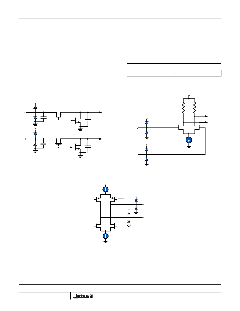
Equivalent Circuits
FIGURE 28. ANALOG INPUTS
FIGURE 29. CLOCK INPUTS
FIGURE 30. LVDS OUTPUTS
AVDD3
INP
INN
AVDD3
F1
F2
Csamp
0.3pF
To
Charge
Pipeline
2pF
F2
Csamp
0.3pF
To
Charge
Pipeline
Φ
AVDD2
CLKP
CLKN
AVDD2
To Clock
Generation
D[9:0]P,
ORP
OVDD
DATA
D[9:0]N,
ORN
OVDD
KAD2710L
相关PDF资料 |
PDF描述 |
|---|---|
| KAD5510P-25Q48 | IC ADC 10BIT CMOS 250MSPS 48QFN |
| KAD5510P-50Q72 | IC ADC 10BIT 500MSPS SGL 72-QFN |
| KAD5512HP-17Q72 | IC ADC 12BIT 170MSPS SGL 72-QFN |
| KAD5512P-17Q72 | IC ADC 12BIT 170MSPS SGL 72-QFN |
| KAD5514P-12Q72 | IC ADC 14BIT 125MSPS SGL 72-QFN |
相关代理商/技术参数 |
参数描述 |
|---|---|
| KAD2710L-27Q68 | 功能描述:IC ADC 10BIT 275MSPS SGL 68-QFN RoHS:是 类别:集成电路 (IC) >> 数据采集 - 模数转换器 系列:FemtoCharge™ 产品培训模块:Lead (SnPb) Finish for COTS Obsolescence Mitigation Program 标准包装:1 系列:- 位数:10 采样率(每秒):357k 数据接口:DSP,MICROWIRE?,QSPI?,串行,SPI? 转换器数目:1 功率耗散(最大):830µW 电压电源:单电源 工作温度:-40°C ~ 85°C 安装类型:表面贴装 封装/外壳:10-WFDFN 裸露焊盘 供应商设备封装:10-TDFN-EP(3x3) 包装:剪切带 (CT) 输入数目和类型:2 个单端,单极;2 个单端,双极;1 个差分,单极;1 个差分,双极 产品目录页面:1396 (CN2011-ZH PDF) 其它名称:MAX1395ETB+TCT |
| KA-D2E | 制造商:Leach International Corporation 功能描述:MID RANGE - Bulk |
| KA-D2F | 制造商:Leach International Corporation 功能描述:EM RLY 4PDT 10A 115VAC SCKT - Bulk |
| KA-D4E | 制造商:Leach International Corporation 功能描述:EM RLY 4PDT 10A 28VAC SCKT - Bulk |
| KA-D4F | 制造商:Leach International Corporation 功能描述:EM RLY 4PDT 10A 115VAC SCKT - Bulk |
发布紧急采购,3分钟左右您将得到回复。