- 您现在的位置:买卖IC网 > PDF目录3990 > KMPC8347ZQAGD (Freescale Semiconductor)IC MPU POWERQUICC II 620-PBGA PDF资料下载
参数资料
| 型号: | KMPC8347ZQAGD |
| 厂商: | Freescale Semiconductor |
| 文件页数: | 75/99页 |
| 文件大小: | 0K |
| 描述: | IC MPU POWERQUICC II 620-PBGA |
| 标准包装: | 2 |
| 系列: | MPC83xx |
| 处理器类型: | 32-位 MPC83xx PowerQUICC II Pro |
| 速度: | 400MHz |
| 电压: | 1.2V |
| 安装类型: | 表面贴装 |
| 封装/外壳: | 620-BBGA 裸露焊盘 |
| 供应商设备封装: | 620-PBGA(29x29) |
| 包装: | 托盘 |
第1页第2页第3页第4页第5页第6页第7页第8页第9页第10页第11页第12页第13页第14页第15页第16页第17页第18页第19页第20页第21页第22页第23页第24页第25页第26页第27页第28页第29页第30页第31页第32页第33页第34页第35页第36页第37页第38页第39页第40页第41页第42页第43页第44页第45页第46页第47页第48页第49页第50页第51页第52页第53页第54页第55页第56页第57页第58页第59页第60页第61页第62页第63页第64页第65页第66页第67页第68页第69页第70页第71页第72页第73页第74页当前第75页第76页第77页第78页第79页第80页第81页第82页第83页第84页第85页第86页第87页第88页第89页第90页第91页第92页第93页第94页第95页第96页第97页第98页第99页
MPC8347EA PowerQUICC II Pro Integrated Host Processor Hardware Specifications, Rev. 12
Freescale Semiconductor
77
Clocking
As shown in Figure 42, the primary clock input (frequency) is multiplied up by the system phase-locked
loop (PLL) and the clock unit to create the coherent system bus clock (csb_clk), the internal clock for the
DDR controller (ddr_clk), and the internal clock for the local bus interface unit (lbiu_clk).
The csb_clk frequency is derived from a complex set of factors that can be simplified into the following
equation:
csb_clk = {PCI_SYNC_IN × (1 + CFG_CLKIN_DIV)} × SPMF
In PCI host mode, PCI_SYNC_IN × (1 + CFG_CLKIN_DIV) is the CLKIN frequency.
The csb_clk serves as the clock input to the e300 core. A second PLL inside the e300 core multiplies the
csb_clk frequency to create the internal clock for the e300 core (core_clk). The system and core PLL
multipliers are selected by the SPMF and COREPLL fields in the reset configuration word low (RCWL),
which is loaded at power-on reset or by one of the hard-coded reset options. See the chapter on reset,
clocking, and initialization in the MPC8349EA Reference Manual for more information on the clock
subsystem.
The internal ddr_clk frequency is determined by the following equation:
ddr_clk = csb_clk × (1 + RCWL[DDRCM])
ddr_clk is not the external memory bus frequency; ddr_clk passes through the DDR clock divider (
÷2) to
create the differential DDR memory bus clock outputs (MCK and MCK). However, the data rate is the
same frequency as ddr_clk.
The internal lbiu_clk frequency is determined by the following equation:
lbiu_clk = csb_clk × (1 + RCWL[LBIUCM])
lbiu_clk is not the external local bus frequency; lbiu_clk passes through the LBIU clock divider to create
the external local bus clock outputs (LSYNC_OUT and LCLK[0:2]). The LBIU clock divider ratio is
controlled by LCCR[CLKDIV].
In addition, some of the internal units may have to be shut off or operate at lower frequency than the
csb_clk frequency. Those units have a default clock ratio that can be configured by a memory-mapped
register after the device exits reset. Table 57 specifies which units have a configurable clock frequency.
Table 58 provides the operating frequencies for the MPC8347EA TBGA under recommended operating
conditions (see Table 2). All frequency combinations shown in the table below may not be available.
Maximum operating frequencies depend on the part ordered, see Section 22.1, “Part Numbers Fully
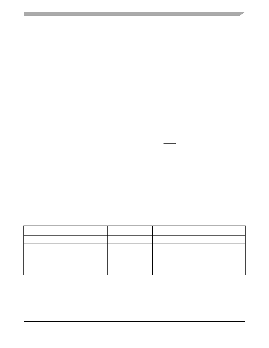
Table 57. Configurable Clock Units
Unit
Default Frequency
Options
TSEC1
csb_clk/3
Off, csb_clk, csb_clk/2, csb_clk/3
TSEC2, I2C1
csb_clk/3
Off, csb_clk, csb_clk/2, csb_clk/3
Security core
csb_clk/3
Off, csb_clk, csb_clk/2, csb_clk/3
USB DR, USB MPH
csb_clk/3
Off, csb_clk, csb_clk/2, csb_clk/3
PCI and DMA complex
csb_clk
Off, csb_clk
相关PDF资料 |
PDF描述 |
|---|---|
| FMC50DREN | CONN EDGECARD 100POS .100 EYELET |
| XC4044XL-1BG432C | IC FPGA C-TEMP 3.3V 1SPD 432MBGA |
| XC4036XL-3HQ240I | IC FPGA I-TEMP 3.3V 3SPD 240HQFP |
| 65801-124LF | CLINCHER RECEPTACLE ASSY TIN |
| FMC50DREH | CONN EDGECARD 100POS .100 EYELET |
相关代理商/技术参数 |
参数描述 |
|---|---|
| KMPC8347ZQAGDB | 功能描述:微处理器 - MPU 8347 PBGA PB W/O ENC RoHS:否 制造商:Atmel 处理器系列:SAMA5D31 核心:ARM Cortex A5 数据总线宽度:32 bit 最大时钟频率:536 MHz 程序存储器大小:32 KB 数据 RAM 大小:128 KB 接口类型:CAN, Ethernet, LIN, SPI,TWI, UART, USB 工作电源电压:1.8 V to 3.3 V 最大工作温度:+ 85 C 安装风格:SMD/SMT 封装 / 箱体:FBGA-324 |
| KMPC8347ZUAGDB | 功能描述:微处理器 - MPU 834X TBGA PB RoHS:否 制造商:Atmel 处理器系列:SAMA5D31 核心:ARM Cortex A5 数据总线宽度:32 bit 最大时钟频率:536 MHz 程序存储器大小:32 KB 数据 RAM 大小:128 KB 接口类型:CAN, Ethernet, LIN, SPI,TWI, UART, USB 工作电源电压:1.8 V to 3.3 V 最大工作温度:+ 85 C 安装风格:SMD/SMT 封装 / 箱体:FBGA-324 |
| KMPC8347ZUAJDB | 功能描述:微处理器 - MPU 8349 TBGA W/PB RoHS:否 制造商:Atmel 处理器系列:SAMA5D31 核心:ARM Cortex A5 数据总线宽度:32 bit 最大时钟频率:536 MHz 程序存储器大小:32 KB 数据 RAM 大小:128 KB 接口类型:CAN, Ethernet, LIN, SPI,TWI, UART, USB 工作电源电压:1.8 V to 3.3 V 最大工作温度:+ 85 C 安装风格:SMD/SMT 封装 / 箱体:FBGA-324 |
| KMPC8347ZUAJF | 功能描述:IC MPU PWRQUICC II 672-TBGA RoHS:否 类别:集成电路 (IC) >> 嵌入式 - 微处理器 系列:MPC83xx 标准包装:2 系列:MPC8xx 处理器类型:32-位 MPC8xx PowerQUICC 特点:- 速度:133MHz 电压:3.3V 安装类型:表面贴装 封装/外壳:357-BBGA 供应商设备封装:357-PBGA(25x25) 包装:托盘 |
| KMPC8347ZUAJFB | 功能描述:微处理器 - MPU 8349 TBGA W/PB RoHS:否 制造商:Atmel 处理器系列:SAMA5D31 核心:ARM Cortex A5 数据总线宽度:32 bit 最大时钟频率:536 MHz 程序存储器大小:32 KB 数据 RAM 大小:128 KB 接口类型:CAN, Ethernet, LIN, SPI,TWI, UART, USB 工作电源电压:1.8 V to 3.3 V 最大工作温度:+ 85 C 安装风格:SMD/SMT 封装 / 箱体:FBGA-324 |
发布紧急采购,3分钟左右您将得到回复。