- 您现在的位置:买卖IC网 > PDF目录3945 > KMPC8377VRALG (Freescale Semiconductor)IC MPU POWERQUICC II 689-PBGA PDF资料下载
参数资料
| 型号: | KMPC8377VRALG |
| 厂商: | Freescale Semiconductor |
| 文件页数: | 104/127页 |
| 文件大小: | 0K |
| 描述: | IC MPU POWERQUICC II 689-PBGA |
| 标准包装: | 2 |
| 系列: | MPC83xx |
| 处理器类型: | 32-位 MPC83xx PowerQUICC II Pro |
| 速度: | 667MHz |
| 电压: | 1V |
| 安装类型: | 表面贴装 |
| 封装/外壳: | 689-BBGA 裸露焊盘 |
| 供应商设备封装: | 689-TEPBGA II(31x31) |
| 包装: | 托盘 |
第1页第2页第3页第4页第5页第6页第7页第8页第9页第10页第11页第12页第13页第14页第15页第16页第17页第18页第19页第20页第21页第22页第23页第24页第25页第26页第27页第28页第29页第30页第31页第32页第33页第34页第35页第36页第37页第38页第39页第40页第41页第42页第43页第44页第45页第46页第47页第48页第49页第50页第51页第52页第53页第54页第55页第56页第57页第58页第59页第60页第61页第62页第63页第64页第65页第66页第67页第68页第69页第70页第71页第72页第73页第74页第75页第76页第77页第78页第79页第80页第81页第82页第83页第84页第85页第86页第87页第88页第89页第90页第91页第92页第93页第94页第95页第96页第97页第98页第99页第100页第101页第102页第103页当前第104页第105页第106页第107页第108页第109页第110页第111页第112页第113页第114页第115页第116页第117页第118页第119页第120页第121页第122页第123页第124页第125页第126页第127页
MPC8377E PowerQUICC II Pro Processor Hardware Specifications, Rev. 8
78
Freescale Semiconductor
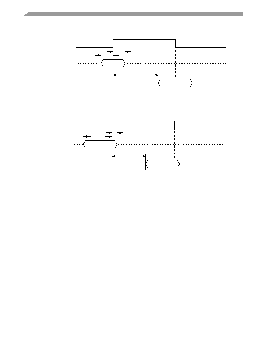
This figure shows the SPI timing in slave mode (external clock).
Figure 49. SPI AC Timing in Slave Mode (External Clock) Diagram
This figure shows the SPI timing in master mode (internal clock).
Figure 50. SPI AC Timing in Master Mode (Internal Clock) Diagram
21 High-Speed Serial Interfaces (HSSI)
This chip features two serializer/deserializer (SerDes) interfaces to be used for high-speed serial
interconnect applications. See Table 1 for the interfaces supported.
This section describes the common portion of SerDes DC electrical specifications, which is the DC
requirement for SerDes reference clocks. The SerDes data lane’s transmitter and receiver reference circuits
are also shown.
21.1
Signal Terms Definition
The SerDes utilizes differential signaling to transfer data across the serial link. This section defines terms
used in the description and specification of differential signals.
Figure 51 shows how the signals are defined. For illustration purpose, only one SerDes lane is used for
description. The figure shows waveform for either a transmitter output (SDn_TX and SDn_TX) or a
receiver input (SDn_RX and SDn_RX). Each signal swings between A volts and B volts where A > B.
SPICLK (input)
tNEIXKH
tNEIVKH
tNEKHOV
Input Signals:
SPIMOSI
(See Note)
Output Signals:
SPIMISO
(See Note)
Note: The clock edge is selectable on SPI.
SPICLK (output)
tNIIXKH
tNIKHOV
Input Signals:
SPIMISO
(See Note)
Output Signals:
SPIMOSI
(See Note)
Note: The clock edge is selectable on SPI.
tNIIVKH
相关PDF资料 |
PDF描述 |
|---|---|
| KMPC8377EVRALG | IC MPU POWERQUICC II 689-PBGA |
| KMPC8377ECVRALG | IC MPU POWERQUICC II 689-PBGA |
| KMPC8377CVRALG | IC MPU POWERQUICC II 689-PBGA |
| KMPC8358VRAGDGA | IC MPU POWERQUICC II 668-PBGA |
| KMPC8358EZQAGDGA | IC MPU POWERQUICC II 668-PBGA |
相关代理商/技术参数 |
参数描述 |
|---|---|
| KMPC8378CVRALG | 功能描述:微处理器 - MPU PBGA W/O ENCR RoHS:否 制造商:Atmel 处理器系列:SAMA5D31 核心:ARM Cortex A5 数据总线宽度:32 bit 最大时钟频率:536 MHz 程序存储器大小:32 KB 数据 RAM 大小:128 KB 接口类型:CAN, Ethernet, LIN, SPI,TWI, UART, USB 工作电源电压:1.8 V to 3.3 V 最大工作温度:+ 85 C 安装风格:SMD/SMT 封装 / 箱体:FBGA-324 |
| KMPC8378ECVRALG | 功能描述:微处理器 - MPU PBGA W/ ENCR RoHS:否 制造商:Atmel 处理器系列:SAMA5D31 核心:ARM Cortex A5 数据总线宽度:32 bit 最大时钟频率:536 MHz 程序存储器大小:32 KB 数据 RAM 大小:128 KB 接口类型:CAN, Ethernet, LIN, SPI,TWI, UART, USB 工作电源电压:1.8 V to 3.3 V 最大工作温度:+ 85 C 安装风格:SMD/SMT 封装 / 箱体:FBGA-324 |
| KMPC8378EVRALG | 功能描述:微处理器 - MPU PBGA W/ ENCR RoHS:否 制造商:Atmel 处理器系列:SAMA5D31 核心:ARM Cortex A5 数据总线宽度:32 bit 最大时钟频率:536 MHz 程序存储器大小:32 KB 数据 RAM 大小:128 KB 接口类型:CAN, Ethernet, LIN, SPI,TWI, UART, USB 工作电源电压:1.8 V to 3.3 V 最大工作温度:+ 85 C 安装风格:SMD/SMT 封装 / 箱体:FBGA-324 |
| KMPC8378VRALG | 功能描述:微处理器 - MPU PBGA W/O ENCR RoHS:否 制造商:Atmel 处理器系列:SAMA5D31 核心:ARM Cortex A5 数据总线宽度:32 bit 最大时钟频率:536 MHz 程序存储器大小:32 KB 数据 RAM 大小:128 KB 接口类型:CAN, Ethernet, LIN, SPI,TWI, UART, USB 工作电源电压:1.8 V to 3.3 V 最大工作温度:+ 85 C 安装风格:SMD/SMT 封装 / 箱体:FBGA-324 |
| KMPC8379CVRALG | 功能描述:微处理器 - MPU PBGA W/O ENCR RoHS:否 制造商:Atmel 处理器系列:SAMA5D31 核心:ARM Cortex A5 数据总线宽度:32 bit 最大时钟频率:536 MHz 程序存储器大小:32 KB 数据 RAM 大小:128 KB 接口类型:CAN, Ethernet, LIN, SPI,TWI, UART, USB 工作电源电压:1.8 V to 3.3 V 最大工作温度:+ 85 C 安装风格:SMD/SMT 封装 / 箱体:FBGA-324 |
发布紧急采购,3分钟左右您将得到回复。