- 您现在的位置:买卖IC网 > PDF目录3945 > KMPC8377VRALG (Freescale Semiconductor)IC MPU POWERQUICC II 689-PBGA PDF资料下载
参数资料
| 型号: | KMPC8377VRALG |
| 厂商: | Freescale Semiconductor |
| 文件页数: | 111/127页 |
| 文件大小: | 0K |
| 描述: | IC MPU POWERQUICC II 689-PBGA |
| 标准包装: | 2 |
| 系列: | MPC83xx |
| 处理器类型: | 32-位 MPC83xx PowerQUICC II Pro |
| 速度: | 667MHz |
| 电压: | 1V |
| 安装类型: | 表面贴装 |
| 封装/外壳: | 689-BBGA 裸露焊盘 |
| 供应商设备封装: | 689-TEPBGA II(31x31) |
| 包装: | 托盘 |
第1页第2页第3页第4页第5页第6页第7页第8页第9页第10页第11页第12页第13页第14页第15页第16页第17页第18页第19页第20页第21页第22页第23页第24页第25页第26页第27页第28页第29页第30页第31页第32页第33页第34页第35页第36页第37页第38页第39页第40页第41页第42页第43页第44页第45页第46页第47页第48页第49页第50页第51页第52页第53页第54页第55页第56页第57页第58页第59页第60页第61页第62页第63页第64页第65页第66页第67页第68页第69页第70页第71页第72页第73页第74页第75页第76页第77页第78页第79页第80页第81页第82页第83页第84页第85页第86页第87页第88页第89页第90页第91页第92页第93页第94页第95页第96页第97页第98页第99页第100页第101页第102页第103页第104页第105页第106页第107页第108页第109页第110页当前第111页第112页第113页第114页第115页第116页第117页第118页第119页第120页第121页第122页第123页第124页第125页第126页第127页
MPC8377E PowerQUICC II Pro Processor Hardware Specifications, Rev. 8
84
Freescale Semiconductor
NOTE
fact that clock driver chip's internal structure, output impedance, and
termination requirements are different between various clock driver chip
manufacturers, it is very possible that the clock circuit reference designs
provided by the clock driver chip vendor are different from what is shown
below. They might also vary from one vendor to the other. Therefore,
Freescale Semiconductor can neither provide the optimal clock driver
reference circuits, nor guarantee the correctness of the following clock
driver connection reference circuits. The system designer is recommended
to contact the selected clock driver chip vendor for the optimal reference
circuits with the device SerDes reference clock receiver requirement
provided in this document.
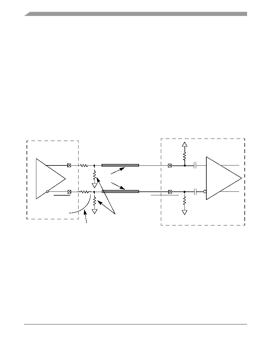
This figure shows the SerDes reference clock connection reference circuits for HCSL type clock driver. It
assumes that the DC levels of the clock driver chip is compatible with device SerDes reference clock
input’s DC requirement.
Figure 56. DC-Coupled Differential Connection with HCSL Clock Driver (Reference Only)
This figure shows the SerDes reference clock connection reference circuits for LVDS type clock driver.
Since LVDS clock driver’s common-mode voltage is higher than the device SerDes reference clock input’s
allowed range (100 to 400 mV), AC-coupled connection scheme must be used. It assumes the LVDS
50
Ω
50
Ω
SD
n_REF_CLK
SD
n_REF_CLK
Clock Driver
100
Ω differential PWB trace
Clock driver vendor dependent
source termination resistor
SerDes Refer.
CLK Receiver
Clock Driver
CLK_Out
HCSL CLK Driver Chip
33
Ω
33
Ω
Total 50
Ω. Assume clock driver’s
output impedance is about 16
Ω.
Chip
CLK_Out
相关PDF资料 |
PDF描述 |
|---|---|
| KMPC8377EVRALG | IC MPU POWERQUICC II 689-PBGA |
| KMPC8377ECVRALG | IC MPU POWERQUICC II 689-PBGA |
| KMPC8377CVRALG | IC MPU POWERQUICC II 689-PBGA |
| KMPC8358VRAGDGA | IC MPU POWERQUICC II 668-PBGA |
| KMPC8358EZQAGDGA | IC MPU POWERQUICC II 668-PBGA |
相关代理商/技术参数 |
参数描述 |
|---|---|
| KMPC8378CVRALG | 功能描述:微处理器 - MPU PBGA W/O ENCR RoHS:否 制造商:Atmel 处理器系列:SAMA5D31 核心:ARM Cortex A5 数据总线宽度:32 bit 最大时钟频率:536 MHz 程序存储器大小:32 KB 数据 RAM 大小:128 KB 接口类型:CAN, Ethernet, LIN, SPI,TWI, UART, USB 工作电源电压:1.8 V to 3.3 V 最大工作温度:+ 85 C 安装风格:SMD/SMT 封装 / 箱体:FBGA-324 |
| KMPC8378ECVRALG | 功能描述:微处理器 - MPU PBGA W/ ENCR RoHS:否 制造商:Atmel 处理器系列:SAMA5D31 核心:ARM Cortex A5 数据总线宽度:32 bit 最大时钟频率:536 MHz 程序存储器大小:32 KB 数据 RAM 大小:128 KB 接口类型:CAN, Ethernet, LIN, SPI,TWI, UART, USB 工作电源电压:1.8 V to 3.3 V 最大工作温度:+ 85 C 安装风格:SMD/SMT 封装 / 箱体:FBGA-324 |
| KMPC8378EVRALG | 功能描述:微处理器 - MPU PBGA W/ ENCR RoHS:否 制造商:Atmel 处理器系列:SAMA5D31 核心:ARM Cortex A5 数据总线宽度:32 bit 最大时钟频率:536 MHz 程序存储器大小:32 KB 数据 RAM 大小:128 KB 接口类型:CAN, Ethernet, LIN, SPI,TWI, UART, USB 工作电源电压:1.8 V to 3.3 V 最大工作温度:+ 85 C 安装风格:SMD/SMT 封装 / 箱体:FBGA-324 |
| KMPC8378VRALG | 功能描述:微处理器 - MPU PBGA W/O ENCR RoHS:否 制造商:Atmel 处理器系列:SAMA5D31 核心:ARM Cortex A5 数据总线宽度:32 bit 最大时钟频率:536 MHz 程序存储器大小:32 KB 数据 RAM 大小:128 KB 接口类型:CAN, Ethernet, LIN, SPI,TWI, UART, USB 工作电源电压:1.8 V to 3.3 V 最大工作温度:+ 85 C 安装风格:SMD/SMT 封装 / 箱体:FBGA-324 |
| KMPC8379CVRALG | 功能描述:微处理器 - MPU PBGA W/O ENCR RoHS:否 制造商:Atmel 处理器系列:SAMA5D31 核心:ARM Cortex A5 数据总线宽度:32 bit 最大时钟频率:536 MHz 程序存储器大小:32 KB 数据 RAM 大小:128 KB 接口类型:CAN, Ethernet, LIN, SPI,TWI, UART, USB 工作电源电压:1.8 V to 3.3 V 最大工作温度:+ 85 C 安装风格:SMD/SMT 封装 / 箱体:FBGA-324 |
发布紧急采购,3分钟左右您将得到回复。