- 您现在的位置:买卖IC网 > PDF目录17725 > L2K110BJ224KB-T (Taiyo Yuden)CAP ARRAY 2CH 0.22UF 10V 0504 PDF资料下载
参数资料
| 型号: | L2K110BJ224KB-T |
| 厂商: | Taiyo Yuden |
| 文件页数: | 13/16页 |
| 文件大小: | 0K |
| 描述: | CAP ARRAY 2CH 0.22UF 10V 0504 |
| 产品变化通告: | X5R, X7R Part Number Change |
| 标准包装: | 10 |
| 电容: | 0.22µF |
| 电压 - 额定: | 10V |
| 电介质材料: | 陶瓷 |
| 电容器数量: | 2 |
| 电路类型: | 隔离 |
| 温度系数: | X5R |
| 容差: | ±10% |
| 安装类型: | 表面贴装 |
| 封装/外壳: | 0504(1210 公制) |
| 尺寸/尺寸: | 0.054" L x 0.039" W(1.37mm x 1.00mm) |
| 高度 - 座高(最大): | 0.024"(0.60mm) |
| 包装: | 剪切带 (CT) |
| 其它名称: | 587-1037-1 |
�� �
�
�■� PRECAUTIONS�
�Precautions� on� the� use� of� Multilayer� Ceramic� Capacitors�
�1.� Circuit� Design�
�◆� Veri?cation� of� operating� environment,� electrical� rating� and� performance�
�1.� A� malfunction� of� equipment� in� ?elds� such� as� medical,� aerospace,� nuclear� control,� etc.� may� cause� serious� harm� to� human� life� or� have� severe� social� rami?cations.�
�Therefore,� any� capacitors� to� be� used� in� such� equipment� may� require� higher� safety� and� reliability,� and� shall� be� clearly� differentiated� from� them� used� in� general� pur-�
�Precautions�
�pose� applications.�
�◆� Operating� Voltage� (� Veri?cation� of� Rated� voltage� )�
�1.� The� operating� voltage� for� capacitors� must� always� be� their� rated� voltage� or� less.�
�If� an� AC� voltage� is� loaded� on� a� DC� voltage,� the� sum� of� the� two� peak� voltages� shall� be� the� rated� voltage� or� less.�
�For� a� circuit� where� an� AC� or� a� pulse� voltage� may� be� used,� the� sum� of� their� peak� voltages� shall� also� be� the� rated� voltage� or� less.�
�2.� Even� if� an� applied� voltage� is� the� rated� voltage� or� less� reliability� of� capacitors� may� be� deteriorated� in� case� that� either� a� high� frequency� AC� voltage� or� a� pulse� voltage�
�having� rapid� rise� time� is� used� in� a� circuit.�
�2.� PCB� Design�
�◆� Pattern� con?gurations� (� Design� of� Land-patterns� )�
�1.� When� capacitors� are� mounted� on� PCBs,� the� amount� of� solder� used� (� size� of� ?llet� )� can� directly� affect� the� capacitor� performance.� Therefore,� the� following� items� must�
�be� carefully� considered� in� the� design� of� land� patterns:�
�(� 1� )� Excessive� solder� applied� can� cause� mechanical� stresses� which� lead� to� chip� breaking� or� cracking.� Therefore,� please� consider� appropriate� land-patterns� for� proper�
�Precautions�
�amount� of� solder.�
�(� 2� )� When� more� than� one� component� are� jointly� soldered� onto� the� same� land,� each� component's� soldering� point� shall� be� separated� by� solder-resist.�
�◆� Pattern� con?gurations� (� Capacitor� layout� on� PCBs� )�
�After� capacitors� are� mounted� on� boards,� they� can� be� subjected� to� mechanical� stresses� in� subsequent� manufacturing� processes� (� PCB� cutting,� board� inspection,�
�mounting� of� additional� parts,� assembly� into� the� chassis,� wave� soldering� of� the� boards,� etc.� )� .� For� this� reason,� land� pattern� con?gurations� and� positions� of� capacitors�
�shall� be� carefully� considered� to� minimize� stresses.�
�◆� Pattern� con?gurations� (� Design� of� Land-patterns� )�
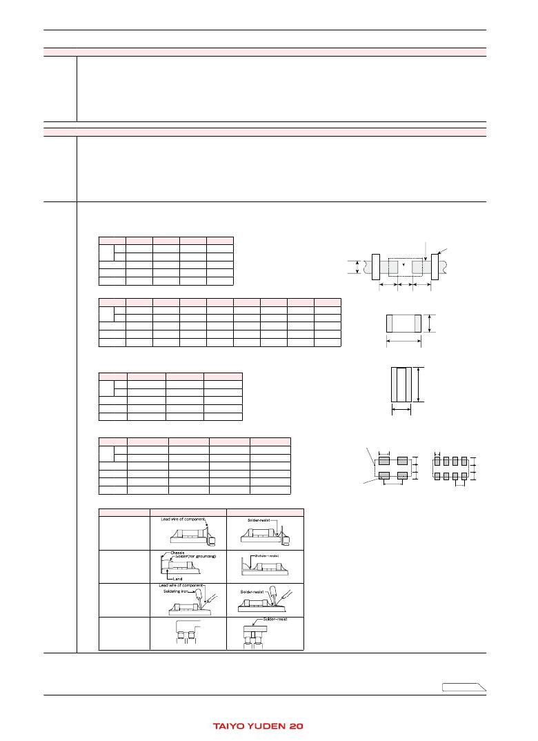
�The� following� diagrams� and� tables� show� some� examples� of� recommended� land� patterns� to� prevent� excessive� solder� amounts.�
�(� 1� )� Recommended� land� dimensions� for� typical� chip� capacitors�
�●� Multilayer� Ceramic� Capacitors� :� Recommended� land� dimensions� (� unit:� mm� )�
� � Wave-soldering� Land� patterns� for� PCBs�
�Type�
�107� 212� 316� 325�
�Land�
�Size�
�A�
�B�
�L�
�W�
�1.6� 2.0� 3.2� 3.2�
�0.8� 5� 1.25� 1.6� 2.5�
�0.8 to 1.0 1.0 to 1.4 1.8 to 2.5 1.8 to 2.5�
�0.5 to 0.8 0.8 to 1.5 0.8 to 1.7 0.8 to 1.7�
�C�
�Chip� capacitor�
�Solder-resist�
�C�
�0.6 to 0.8 0.9 to 1.2 1.2 to 1.6 1.8 to 2.5�
�Re?ow-soldering�
�B�
�A�
�B�
�Type�
�042� 063� 105� 107�
�212�
�316�
�325�
�432�
�Size�
�A�
�L�
�W�
�0.4� 0.6� 1.0� 1.6�
�0.2� 0.3� 0.5� 0.8�
�0.15 to 0.25 0.20 to 0.30 0.45 to 0.55� 0.8� to� 1.0�
�2.0�
�5� 1.25�
�0.8� to� 1.2�
�3.2�
�1.6�
�1.8� to� 2.5�
�3.2�
�2.5�
�1.8� to� 2.5�
�4.5�
�3.2�
�2.5� to� 3.5�
�Chip� capacitor�
�W�
�B�
�0.15 to 0.20 0.20 to 0.30 0.40 to 0.50� 0.6� to� 0.8�
�0.8� to� 1.2�
�1.0� to� 1.5�
�1.0� to� 1.5�
�1.5� to� 1.8�
�C� 0.15 to 0.30 0.25 to 0.40 0.45 to 0.55� 0.6� to� 0.8� 0.9� to� 1.6� 1.2� to� 2.0� 1.8� to� 3.2� 2.3� to� 3.5�
�Note� :� Recommended� land� size� might� be� different� according� to� the� allowance� of� the� size� of� the� product.�
�●� LWDC:� Recommended� land� dimensions� for� re?ow-soldering� (� unit:� mm� )�
�L�
�LWDC�
�Type�
�105�
�107�
�212�
�Size�
�A�
�L�
�W�
�0.52�
�1.0�
�0.18� to� 0.22�
�5� 0.8�
�1.6�
�0.25� to� 0.3�
�1.25�
�2.0�
�0.5� to� 0.7�
�W�
�Technical�
�B�
�C�
�0.2� to� 0.25�
�0.9� to� 1.1�
�0.3� to� 0.4�
�1.5� to� 1.7�
�0.4� to� 0.5�
�1.9� to� 2.1�
�L�
�consider-�
�ations�
�(�
�●� Array� type:� Recommended� land� dimensions� for� re?ow-soldering� (� unit:� mm� )�
�Type� 096� (� 2 circuits� )� 110� (� 2� circuits� )� 212� (� 2� circuits� )� 212� 4� circuits� )�
�L� 0.9� 1.37� 2.0� 2.0�
�Size�
�W� 0.6� 1.0� 1.25� 1.25�
�a� 0.25� to� 0.35� 0.35� to� 0.45� 0.5� to� 0.6� 0.5� to� 0.6�
�b� 0.15� to� 0.25� 0.55� to� 0.65� 0.5� to� 0.6� 0.5� to� 0.6�
�c�
�0.15� to� 0.25� 0.3� to� 0.4� 0.5� to� 0.6� 0.2� to� 0.3�
�d�
�0.45� 0.64� 1.0� 0.5�
�2� circuits�
�Chip� capacitor�
�Land�
�c�
�d�
�a�
�b�
�a�
�4� circuits�
�c�
�d�
�a�
�b�
�a�
�(� 2� )� Examples� of� good� and� bad� solder� application�
�Items�
�Not� recommended�
�Recommended�
�Mixed� mounting� of�
�SMD� and� leaded�
�components�
�Component�
�placement� close� to�
�the� chassis�
�Hand-soldering�
�of� leaded�
�components�
�near� mounted�
�components�
�Horizontal�
�component�
�placement�
�To� next� page�
�*� This� catalog� contains� the� typical� speci� ?cation� only� due� to� the� limitation� of� space.� When� you� consider� the� purchase� of� our� products,� please� check� our� speci� ?cation.�
�For� details� of� each� product� (characteristics� graph,� reliability� information,� precautions� for� use,� and� so� on),� see� our� Web� site� (http://www.ty-top.com/)� or� CD� catalogs.�
�mlcc_prec-P1�
�12�
�mlcc_prec_e-01�
�相关PDF资料 |
PDF描述 |
|---|---|
| E2K212BJ105KD-T | CAP ARRAY 2CH 1UF 16V 0805 |
| MB2411S2W13 | SWITCH PUSHBUTTON SPDT 3A 125V |
| BDH107 | HANDLE PISTOL 2.6" RED/YELLOW |
| MB2411A1W01-HC | SWITCH PUSHBUTTON SPDT 3A 125V |
| SFELF10M7HA00-A0 | FILTER 10.7MHZ 180KHZ BAND RADIA |
相关代理商/技术参数 |
参数描述 |
|---|---|
| L2K110BJ474KA-T | 功能描述:电容器阵列与网络 CAP ARRAY 0504 10V X5R .047uF 20% RoHS:否 制造商:AVX 电容:0.1 uF 容差:20 % 电压额定值:6.3 V 元件数量:2 工作温度范围: 外壳长度:0.8 mm 外壳宽度:1.6 mm 外壳高度:0.5 mm 端接类型:SMD/SMT 系列:PG |
| L2K212BJ105KD-T | 功能描述:电容器阵列与网络 CAP ARRAY 0805 10V X5R 1uF 10% RoHS:否 制造商:AVX 电容:0.1 uF 容差:20 % 电压额定值:6.3 V 元件数量:2 工作温度范围: 外壳长度:0.8 mm 外壳宽度:1.6 mm 外壳高度:0.5 mm 端接类型:SMD/SMT 系列:PG |
| L2K212BJ105MD-T | 功能描述:电容器阵列与网络 CAP ARRAY 0805 10V X5R 1uF 20% RoHS:否 制造商:AVX 电容:0.1 uF 容差:20 % 电压额定值:6.3 V 元件数量:2 工作温度范围: 外壳长度:0.8 mm 外壳宽度:1.6 mm 外壳高度:0.5 mm 端接类型:SMD/SMT 系列:PG |
| L2K212BJ225MD-T | 功能描述:电容器阵列与网络 CAP ARRAY 0805 X5R 2.2uF 20% RoHS:否 制造商:AVX 电容:0.1 uF 容差:20 % 电压额定值:6.3 V 元件数量:2 工作温度范围: 外壳长度:0.8 mm 外壳宽度:1.6 mm 外壳高度:0.5 mm 端接类型:SMD/SMT 系列:PG |
| L-2K2-F1-352 | 制造商:Ohmite Mfg Co 功能描述: |
发布紧急采购,3分钟左右您将得到回复。