- 您现在的位置:买卖IC网 > PDF目录43899 > L5993D013TR (STMICROELECTRONICS) 1.5 A SWITCHING REGULATOR, 1000 kHz SWITCHING FREQ-MAX, PDSO16 PDF资料下载
参数资料
| 型号: | L5993D013TR |
| 厂商: | STMICROELECTRONICS |
| 元件分类: | 稳压器 |
| 英文描述: | 1.5 A SWITCHING REGULATOR, 1000 kHz SWITCHING FREQ-MAX, PDSO16 |
| 封装: | SO-16 |
| 文件页数: | 4/22页 |
| 文件大小: | 200K |
| 代理商: | L5993D013TR |
Pin 12. SGND (Signal Ground). This ground refer-
ences the control circuitry of the IC, so all the
ground connections of the external parts related
to control functions must lead to this pin. In laying
out the PCB, care must be taken in preventing
switched high currents from flowing through the
SGND path.
Pin 13. ISEN (Current Sense). This pin is to be
connected to the ”hot” lead of the current sense
resistor Rsense (being the other one grounded), to
get a voltage ramp which is an image of the cur-
rent of the switch (IQ). When this voltage is equal
to:
V13pk = IQpk Rsense =
VCOMP
1.4
3
(8)
the conduction of the switch is terminated.
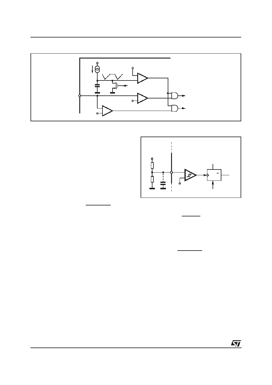
To increase the noise immunity, a ”Leading Edge
Blanking” of about 100ns is internally realized as
shown in fig. 27. Because of that, the smoothing
RC filter between this pin and Rsense could be re-
moved or, at least, considerably reduced.
Pin 14. DIS (Device Disable). When the voltage
on pin 14 rises above 2.5V the IC is shut down
and it is necessary to pull VCC (IC supply voltage,
pin 8) below the UVLO threshold to allow the de-
vice to restart.
The pin can be driven by an external logic signal
in case of power management, as shown in fig.
28. It is also possible to realize an overvoltage
protection, as shown in the section ” Application
Ideas”.If used, bypass this pin to ground with a fil-
ter capacitor to avoid spurious activation due to
noise spikes. If not, it must be connected to
SGND.
Pin 15. DC-LIM (Maximum Duty Cycle Limit). The
upper extreme, Dx, of the duty cycle range de-
pends on the voltage applied to this pin. Approxi-
mately,
Dx
RT
+ 230
(9
)
if DC-LIM is grounded or left floating. Instead,
connecting DC-LIM to VREF (half duty cycle op-
tion), Dx will be set approximately to:
Dx
RT
2
RT + 260
(10)
and the output switching frequency will be halved
with respect to the oscillator one because an in-
ternal T flip-flop (see block diagram, fig. 1) is acti-
vated. Fig. 29 shows the operation.
The half duty cycle option speeds up the dis-
charge of the timing capacitor CT (in order to get
duty cycles as close as possible to 50%) so the
oscillator frequency - with the same RT and CT -
will be slightly higher.
The halving of frequency can be used to reduce
losses at light load in all those systems that must
comply with requirements regarding energy con-
sumption (e.g. monitor displays, see ”Application
Ideas”).
+
-
I
D97IN503
ISEN
0
3V
CLK
2V
+
-
+
-
1.2V
FROM E/A
OVERCURRENT
COMPARATOR
PWM
COMPARATOR
TO PWM
LOGIC
TO FAULT
LOGIC
13
Figure 27. Internal LEB.
+
-
C
D97IN502
DIS
D
R
Q
DISABLE
UVLO
2.5V
14
DISABLE
SIGNAL
Figure 28. Disable (Latched)
L5993
12/22
相关PDF资料 |
PDF描述 |
|---|---|
| L5993 | 1.5 A SWITCHING REGULATOR, 1000 kHz SWITCHING FREQ-MAX, PDIP16 |
| L6115 | QUAD 1-CHANNEL, SGL POLE SGL THROW SWITCH, PZFM15 |
| L6114 | QUAD 1-CHANNEL, SGL POLE SGL THROW SWITCH, PDIP20 |
| L6205PD | STEPPER MOTOR CONTROLLER, 5.6 A, PDSO20 |
| L6205D013TR | STEPPER MOTOR CONTROLLER, 5.6 A, PDSO20 |
相关代理商/技术参数 |
参数描述 |
|---|---|
| L5994 | 功能描述:电流型 PWM 控制器 Adj Triple Out Pwr RoHS:否 制造商:Texas Instruments 开关频率:27 KHz 上升时间: 下降时间: 工作电源电压:6 V to 15 V 工作电源电流:1.5 mA 输出端数量:1 最大工作温度:+ 105 C 安装风格:SMD/SMT 封装 / 箱体:TSSOP-14 |
| L5994_02 | 制造商:STMICROELECTRONICS 制造商全称:STMicroelectronics 功能描述:ADJUSTABLE TRIPLE OUTPUT POWER SUPPLY CONTROLLER |
| L5994A | 功能描述:监控电路 ADJT TRIPLE OUTPUT POWER SUPPLY CNTLR RoHS:否 制造商:STMicroelectronics 监测电压数: 监测电压: 欠电压阈值: 过电压阈值: 输出类型:Active Low, Open Drain 人工复位:Resettable 监视器:No Watchdog 电池备用开关:No Backup 上电复位延迟(典型值):10 s 电源电压-最大:5.5 V 最大工作温度:+ 85 C 安装风格:SMD/SMT 封装 / 箱体:UDFN-6 封装:Reel |
| L5995 | 制造商:未知厂家 制造商全称:未知厂家 功能描述:Current-Mode SMPS Controller |
| L5996 | 制造商:STMICROELECTRONICS 制造商全称:STMicroelectronics 功能描述:5 BIT DYNAMIC DAC CONTROLLER FOR MOBILE CPU |
发布紧急采购,3分钟左右您将得到回复。