- 您现在的位置:买卖IC网 > PDF目录95588 > L6219DS STEPPER MOTOR CONTROLLER, 1 A, PDSO24 PDF资料下载
参数资料
| 型号: | L6219DS |
| 元件分类: | 运动控制电子 |
| 英文描述: | STEPPER MOTOR CONTROLLER, 1 A, PDSO24 |
| 封装: | SOIC-24 |
| 文件页数: | 1/8页 |
| 文件大小: | 961K |
| 代理商: | L6219DS |
DUAL FULL-BRIDGE
PWM MOTOR DRIVER
The L6219DS motor driver is designed to drive both windings of a
bipolar stepper motor or bidirectionally control two dc motors. Both
bridges are capable of sustaining 45 V and include internal pulse-width
modulation (PWM) control of the output current to 750 mA. The outputs
have been optimized for a low output saturation voltage drop (less than
1.8 V total source plus sink at 500 mA).
For PWM current control, the maximum output current is deter-
mined by the user’s selection of a reference voltage and sensing
resistor. Two logic-level inputs select output current limits of 0, 33,
67, or 100% of the maximum level. A PHASE input to each bridge
determines load current direction.
The bridges include both ground clamp and flyback diodes for
protection against inductive transients. Internally generated delays
prevent cross-over currents when switching current direction. Special
power-up sequencing is not required. Thermal protection circuitry
disables the outputs if the chip temperature exceeds safe operating
limits.
The L6219DS is supplied in a 24-pin surface-mountable SOIC. Its
batwing construction provides for maximum package power dissipation
in the smallest possible construction. This device is also available on
special order for operation from -40°C to +85°C or to +105°C. A lead-
free version (100% matte tin leadframe) is also available.
FEATURES
■
Interchangeable with SGS L6219DS
■
750 mA Continuous Output Current
■
45 V Output Sustaining Voltage
■
Internal Clamp Diodes
■
Internal PWM Current Control
■
Low Output Saturation Voltage
■
Internal Thermal Shutdown Circuitry
■
Similar to Dual PBL3717, UC3770
Data
Sheet
29319.43G
L6219DS
ABSOLUTE MAXIMUM RATINGS
at T
J≤
≤≤≤≤ 150°C
Motor Supply Voltage, V
BB
.................... 45 V
Output Current, I
OUT
(Peak) ........................................ +1.0 A
(Continuous) .......................... +750 mA
Logic Supply Voltage, V
CC
................... 7.0 V
Logic Input Voltage Range,
V
IN
......................... -0.3 V to V
CC
+0.3 V
Output Emitter Voltage, V
SENSE
............ 1.5 V
Package Power Dissipation,
P
D
........................................................
See Graph
Operating Temperature Range,
T
A
................................. -20°C to +85°C
Storage Temperature Range,
T
S
............................... -55°C to +150°C
Output current rating may be limited by duty
cycle, ambient temperature, and heat sinking.
Under any set of conditions, do not exceed the
specified peak current rating or a junction
temperature of +150°C.
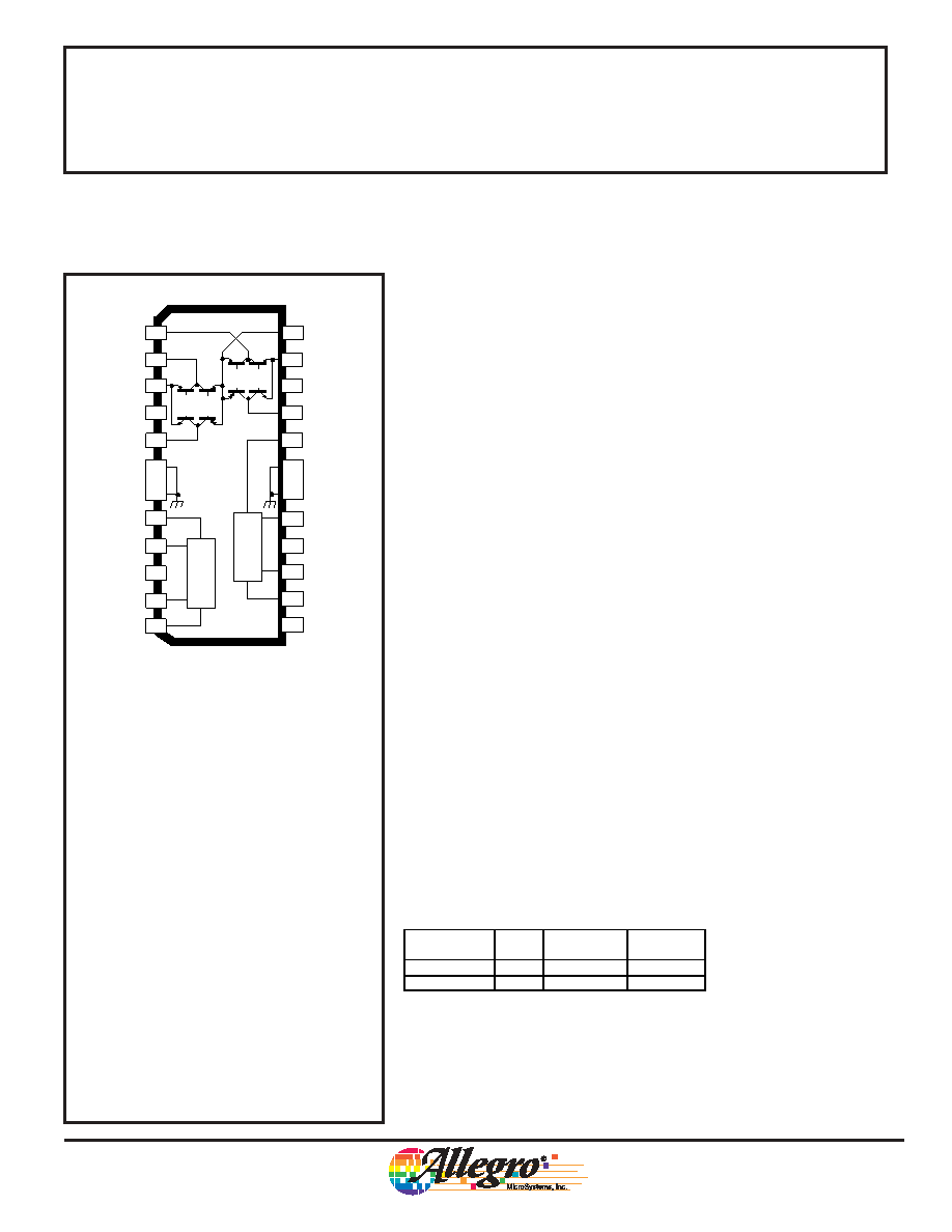
1
2
3
4
5
6
7
8
9
24
23
22
21
20
19
18
17
16
15
14
13
12
11
10
9
θ
2
θ1
VCC
PWM
2
PWM
1
2
VBB
1
GROUND
02
I
12
I
PHASE 2
V REF 2
2
RC
1
RC
V REF 1
PHASE 1
11
I
2B
OUT
SENSE 2
2
COMP IN
2A
OUT
1A
OUT
1
COMP IN
SENSE 1
1B
OUT
01
I
LOAD
SUPPLY
LOGIC
SUPPLY
Dwg. PP-005-3
Part Number
Pb-free*
Package
Packing
L6219DS-T
Yes
24-pin SOIC
31 per tube
L6219DSTR-T
Yes
24-pin SOIC
1000 per reel
*Pb-based variants are being phased out of the product line. The variants cited in this
footnote are in production but have been determined to be LAST TIME BUY. This
classification indicates that sale of this device is currently restricted to existing
customer applications. The variants should not be purchased for new design
applications because obsolescence in the near future is probable. Samples are no
longer available. Status change: October 31, 2006. Deadline for receipt fo LAST TIME
BUY orders: April 27, 2007. These variants include:L6219DS and
L6219DSTR.
相关PDF资料 |
PDF描述 |
|---|---|
| L6219DSTR | STEPPER MOTOR CONTROLLER, 1 A, PDSO24 |
| L6234D | BRUSHLESS DC MOTOR CONTROLLER, 2.5 A, PDSO20 |
| L6243DS | VOICE COIL MOTOR CONTROLLER, 1.2 A, PDSO24 |
| L6287 | SPECIALTY ANALOG CIRCUIT, PDIP42 |
| L6670 | SPECIALTY ANALOG CIRCUIT, PDSO24 |
相关代理商/技术参数 |
参数描述 |
|---|---|
| L6219DS013TR | 功能描述:马达/运动/点火控制器和驱动器 Dual Stepper Motor RoHS:否 制造商:STMicroelectronics 产品:Stepper Motor Controllers / Drivers 类型:2 Phase Stepper Motor Driver 工作电源电压:8 V to 45 V 电源电流:0.5 mA 工作温度:- 25 C to + 125 C 安装风格:SMD/SMT 封装 / 箱体:HTSSOP-28 封装:Tube |
| L6219DS013TRE | 制造商:STMicroelectronics 功能描述: |
| L6219DSA | 功能描述:马达/运动/点火控制器和驱动器 Dual Stepper Motor RoHS:否 制造商:STMicroelectronics 产品:Stepper Motor Controllers / Drivers 类型:2 Phase Stepper Motor Driver 工作电源电压:8 V to 45 V 电源电流:0.5 mA 工作温度:- 25 C to + 125 C 安装风格:SMD/SMT 封装 / 箱体:HTSSOP-28 封装:Tube |
| L6219DSA_08 | 制造商:STMICROELECTRONICS 制造商全称:STMicroelectronics 功能描述:Stepper motor driver for automotive range |
| L6219DSA13TR | 功能描述:马达/运动/点火控制器和驱动器 Dual Stepper Motor RoHS:否 制造商:STMicroelectronics 产品:Stepper Motor Controllers / Drivers 类型:2 Phase Stepper Motor Driver 工作电源电压:8 V to 45 V 电源电流:0.5 mA 工作温度:- 25 C to + 125 C 安装风格:SMD/SMT 封装 / 箱体:HTSSOP-28 封装:Tube |
发布紧急采购,3分钟左右您将得到回复。