- 您现在的位置:买卖IC网 > PDF目录79836 > L6599ADTR (STMICROELECTRONICS) SWITCHING CONTROLLER, PDSO16 PDF资料下载
参数资料
| 型号: | L6599ADTR |
| 厂商: | STMICROELECTRONICS |
| 元件分类: | 稳压器 |
| 英文描述: | SWITCHING CONTROLLER, PDSO16 |
| 封装: | ROHS COMPLIANT, SOP-16 |
| 文件页数: | 34/36页 |
| 文件大小: | 1595K |
| 代理商: | L6599ADTR |
第1页第2页第3页第4页第5页第6页第7页第8页第9页第10页第11页第12页第13页第14页第15页第16页第17页第18页第19页第20页第21页第22页第23页第24页第25页第26页第27页第28页第29页第30页第31页第32页第33页当前第34页第35页第36页
L6599A
Pin connection
Doc ID 15308 Rev 5
7/36
9PFC_STOP
Open-drain ON/OFF control of PFC controller. This pin, normally open, is
intended for stopping the PFC controller, for protection purpose or during
burst-mode operation. It goes low when the IC is shut down by DIS>1.85 V,
ISEN > 1.5 V, LINE > 6 V and STBY < 1.24 V. The pin is pulled low also
when the voltage on pin DELAY exceeds 2 V and goes back open as the
voltage falls below 0.3 V. During UVLO, it is open. Leave the pin
unconnected if not used.
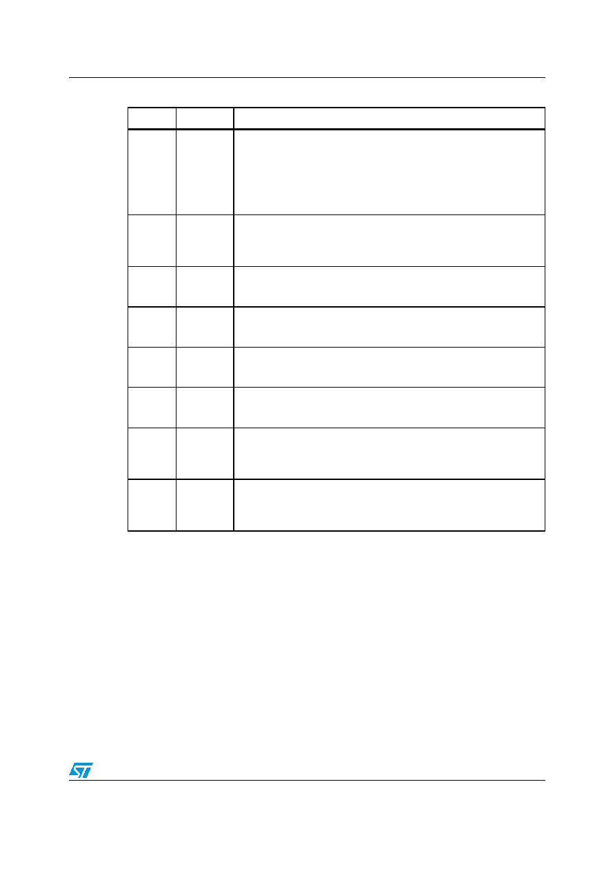
10
GND
Chip ground. Current return for both the low-side gate-drive current and
the bias current of the IC. All of the ground connections of the bias
components should be tied to a track going to this pin and kept separate
from any pulsed current return.
11
LVG
Low-side gate-drive output. The driver is capable of 0.3 A min. source and
0.8 A min. sink peak current to drive the lower MOSFET of the half-bridge
leg. The pin is actively pulled to GND during UVLO.
12
Vcc
Supply voltage of both the signal part of the IC and the low-side gate
driver. Sometimes a small bypass capacitor (0.1 F typ.) to GND might be
useful to get a clean bias voltage for the signal part of the IC.
13
N.C.
High-voltage spacer. The pin is not internally connected to isolate the high-
voltage pin and ease compliance with safety regulations (creepage
distance) on the PCB.
14
OUT
High-side gate-drive floating ground. Current return for the high-side gate-
drive current. Layout carefully the connection of this pin to avoid too large
spikes below ground.
15
HVG
High-side floating gate-drive output. The driver is capable of 0.3 A min.
source and 0.8 A min. sink peak current to drive the upper MOSFET of the
half-bridge leg. A resistor internally connected to pin 14 (OUT) ensures
that the pin is not floating during UVLO.
16
VBOOT
High-side gate-drive floating supply Voltage. The bootstrap capacitor
connected between this pin and pin 14 (OUT) is fed by an internal
synchronous bootstrap diode driven in-phase with the low-side gate-drive.
This patented structure replaces the normally used external diode.
Table 2.
Pin description (continued)
Pin N#
Type
Function
相关PDF资料 |
PDF描述 |
|---|---|
| LFA28DP | 2-OUTPUT 75 W DC-DC REG PWR SUPPLY MODULE |
| LM2576T-12 | 7.5 A SWITCHING REGULATOR, 62 kHz SWITCHING FREQ-MAX, PSFM5 |
| LS4501-7ERD0TB1 | 1-OUTPUT 100 W AC-DC PWR FACTOR CORR MODULE |
| LS4501-7ERD1TB1 | 1-OUTPUT 100 W AC-DC PWR FACTOR CORR MODULE |
| LS4601-7ERD0TB1 | 1-OUTPUT 100 W AC-DC PWR FACTOR CORR MODULE |
相关代理商/技术参数 |
参数描述 |
|---|---|
| L6599AFD | 功能描述:Power Supply Controller Resonant Converter Controller 16-SO 制造商:stmicroelectronics 系列:- 包装:管件 零件状态:有效 应用:谐振转换器控制器 电压 - 输入:- 电压 - 电源:8.85 V ~ 16 V 电流 - 电源:3.5mA 工作温度:-50°C ~ 125°C 安装类型:表面贴装 封装/外壳:16-SOIC(0.154",3.90mm 宽) 供应商器件封装:16-SO 标准包装:50 |
| L6599AN | 功能描述:电压模式 PWM 控制器 Hi-Volt resonant controller, 500KHz RoHS:否 制造商:Texas Instruments 输出端数量:1 拓扑结构:Buck 输出电压:34 V 输出电流: 开关频率: 工作电源电压:4.5 V to 5.5 V 电源电流:600 uA 最大工作温度:+ 125 C 最小工作温度:- 40 C 封装 / 箱体:WSON-8 封装:Reel |
| L6599ATD | 功能描述:电压模式 PWM 控制器 Sgl Output 13.3 V 200 KHz SOIC-16 Nrw RoHS:否 制造商:Texas Instruments 输出端数量:1 拓扑结构:Buck 输出电压:34 V 输出电流: 开关频率: 工作电源电压:4.5 V to 5.5 V 电源电流:600 uA 最大工作温度:+ 125 C 最小工作温度:- 40 C 封装 / 箱体:WSON-8 封装:Reel |
| L6599ATDTR | 功能描述:开关变换器、稳压器与控制器 IMPROVED High-Volt RESONANT CONTROLLER RoHS:否 制造商:Texas Instruments 输出电压:1.2 V to 10 V 输出电流:300 mA 输出功率: 输入电压:3 V to 17 V 开关频率:1 MHz 工作温度范围: 安装风格:SMD/SMT 封装 / 箱体:WSON-8 封装:Reel |
| L6599ATN | 制造商:STMicroelectronics 功能描述: |
发布紧急采购,3分钟左右您将得到回复。