- 您现在的位置:买卖IC网 > PDF目录69003 > L6710 (STMICROELECTRONICS) 2 A SWITCHING CONTROLLER, PQFP44 PDF资料下载
参数资料
| 型号: | L6710 |
| 厂商: | STMICROELECTRONICS |
| 元件分类: | 稳压器 |
| 英文描述: | 2 A SWITCHING CONTROLLER, PQFP44 |
| 封装: | 10 X 10 MM, 1 MM HEIGHT, TQFP-44 |
| 文件页数: | 20/34页 |
| 文件大小: | 1610K |
| 代理商: | L6710 |
第1页第2页第3页第4页第5页第6页第7页第8页第9页第10页第11页第12页第13页第14页第15页第16页第17页第18页第19页当前第20页第21页第22页第23页第24页第25页第26页第27页第28页第29页第30页第31页第32页第33页第34页
27/34
L6710
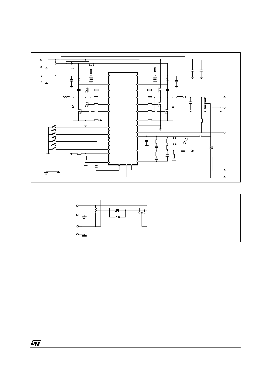
Figure 20. Demo Board Schematic
Figure 21. Power supply configuration
Two main configurations can be distinguished: Single Supply (VCC=VIN=12V) and Double Supply
(VCC=12V VIN=5V or different).
– Single Supply: In this case JP6 has to be completely shorted. The device is supplied with the same
rail that is used for the conversion. With an additional zener diode DZ1 a lower voltage can be derived
to supply the mosfets driver if Logic level mosfet are used. In this case JP1 must be left open so that
the HS driver is supplied with VIN-VDZ1 through BOOTx and JP2 must be shorted to the left to use
VIN or to the right to use VIN-VDZ1 to supply the LS driver through VCCDR pin. Otherwise, JP1 must
be shorted and JP2 can be freely shorted in one of the two positions.
– Double Supply: In this case VCC supply directly the controller (12V) while VIN supplies the HS drains
for the power conversion. This last one can start indifferently from the 5V bus (Typ.) or from other
buses allowing maximum flexibility in the power conversion. Supply for the mosfet driver can be pro-
grammed through the jumpers JP1, JP2 and JP6 as previously illustrated. JP6 selects now VCC or
VIN depending on the requirements.
Some examples are reported in the following Figures 22 and 23.
L6710
U1
PGOOD
PGND
PGNDS
ISEN2
LGATE2
VSEN
FB
PHASE2
UGATE2
BOOT2
VCC
COMP
SGND
OSC
VID0
VID1
VID2
VID3
VID4
ISEN1
LGATE1
PHASE1
UGATE1
BOOT1
VCCDR
5
31
35
36
38
21
20
41
3
43
42
40
19
28
27
26
24
25
6, 7
39
30
13
9
8
17
18
FBR
FBG
22
C1
R8
C2
R4
R3
Q3
Q4
C3
L2
C7
R11
D3
C6
C11..C14
C15,
C24
R1
JP3
R2
S1
S0
S3
S2
S4
R5
R6
Q1
L1
Q2
C4
D4
C5
Vin
GNDin
GNDCORE
VoutCORE
PGOOD
FBG
FBR
DZ1
C8
JP2
JP1
R13
R15
R12
R14
C9,C10
R9
R18
D1
R17
R16
Q1a
Q3a
D2
R19
R20
JP5
JP4
Vcc
GNDcc
JP6
To
Vcc pin
R21
VID5
29
S5
14
REF_OUT
12
OUTEN
To
PGNDS
C25
R10
L6710 EVALUATION BOARD REV.1
NTC1
R22
To
Vcc pin
C26
OUTEN
R7a
R7
JP7
JP8
C28
Vin
GNDin
DZ1
JP2
JP1
Vcc
GNDcc
JP6
To Vcc pin
To HS Drains (Power Input)
To BOOTx (HS Driver Supply)
To VCCDR pin (LS Driver Supply)
相关PDF资料 |
PDF描述 |
|---|---|
| L6710TR | 2 A SWITCHING CONTROLLER, PQFP44 |
| L6713ATR | 2 A SWITCHING CONTROLLER, 225 kHz SWITCHING FREQ-MAX, PQFP64 |
| L6716TR | DUAL SWITCHING CONTROLLER, 225 kHz SWITCHING FREQ-MAX, QCC48 |
| L6716 | DUAL SWITCHING CONTROLLER, 225 kHz SWITCHING FREQ-MAX, QCC48 |
| L6722 | SWITCHING CONTROLLER, 300 kHz SWITCHING FREQ-MAX, QCC36 |
相关代理商/技术参数 |
参数描述 |
|---|---|
| L6710TR | 功能描述:功率驱动器IC 6-Bit Dual Ph Contlr RoHS:否 制造商:Micrel 产品:MOSFET Gate Drivers 类型:Low Cost High or Low Side MOSFET Driver 上升时间: 下降时间: 电源电压-最大:30 V 电源电压-最小:2.75 V 电源电流: 最大功率耗散: 最大工作温度:+ 85 C 安装风格:SMD/SMT 封装 / 箱体:SOIC-8 封装:Tube |
| L6711 | 功能描述:DC/DC 开关控制器 3 PHASE CONTROLLER RoHS:否 制造商:Texas Instruments 输入电压:6 V to 100 V 开关频率: 输出电压:1.215 V to 80 V 输出电流:3.5 A 输出端数量:1 最大工作温度:+ 125 C 安装风格: 封装 / 箱体:CPAK |
| L6711_06 | 制造商:STMICROELECTRONICS 制造商全称:STMicroelectronics 功能描述:3 Phase controller with dynamic VID and selectable DACs |
| L6711TR | 功能描述:DC/DC 开关控制器 3 PHASE CONTROLLER RoHS:否 制造商:Texas Instruments 输入电压:6 V to 100 V 开关频率: 输出电压:1.215 V to 80 V 输出电流:3.5 A 输出端数量:1 最大工作温度:+ 125 C 安装风格: 封装 / 箱体:CPAK |
| L6712 | 制造商:STMICROELECTRONICS 制造商全称:STMicroelectronics 功能描述:TWO-PHASE INTERLEAVED DC/DC CONTROLLER |
发布紧急采购,3分钟左右您将得到回复。