- 您现在的位置:买卖IC网 > PDF目录97995 > L6911ETR (STMICROELECTRONICS) 1.3 A SWITCHING CONTROLLER, 1000 kHz SWITCHING FREQ-MAX, PDSO20 PDF资料下载
参数资料
| 型号: | L6911ETR |
| 厂商: | STMICROELECTRONICS |
| 元件分类: | 稳压器 |
| 英文描述: | 1.3 A SWITCHING CONTROLLER, 1000 kHz SWITCHING FREQ-MAX, PDSO20 |
| 封装: | SO-20 |
| 文件页数: | 8/34页 |
| 文件大小: | 558K |
| 代理商: | L6911ETR |
第1页第2页第3页第4页第5页第6页第7页当前第8页第9页第10页第11页第12页第13页第14页第15页第16页第17页第18页第19页第20页第21页第22页第23页第24页第25页第26页第27页第28页第29页第30页第31页第32页第33页第34页
Obsolete
Product(s)
- Obsolete
Product(s)
Obsolete
Product(s)
- Obsolete
Product(s)
Device description
L6911E
16/34
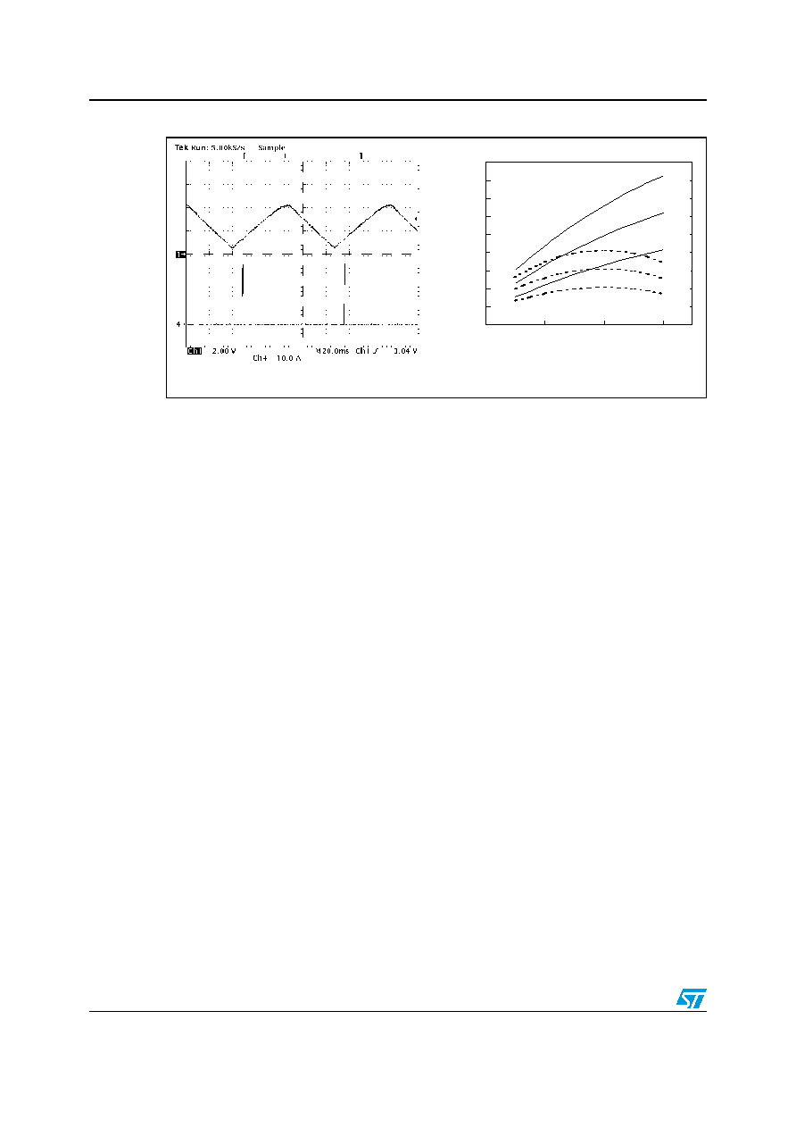
Figure 7.
Hiccup mode and Inductor ripple current vs. VOUT
5.6
Inductor design
The inductance value is defined by a compromise between the transient response time, the
efficiency, the cost and the size. The inductor has to be calculated to sustain the output and
the input voltage variation to maintain the ripple current
I
L between 20% and 30% of the
maximum output current. The inductance value can be calculated with this relationship:
Equation 6
Where fSW is the switching frequency, VIN is the input voltage and VOUT is the output
voltage. Figure 7 b shows the ripple current vs. the output voltage for different values of the
inductor, with vin = 5V and Vin = 12V.
Increasing the value of the inductance reduces the ripple current but, at the same time,
reduces the converter response time to a load transient. If the compensation network is well
designed, the device is able to open or close the duty cycle up to 100% or down to 0%. The
response time is now the time required by the inductor to change its current from initial to
final value. Since the inductor has not finished its charging time, the output current is
supplied by the output capacitors. Minimizing the response time can minimize the output
capacitance required.
The response time to a load transient is different for the application or the removal of the
load: if during the application of the load the inductor is charged by a voltage equal to the
difference between the input and the output voltage, during the removal it is discharged only
by the output voltage. The following expressions give approximate response time for
I load
transient in case of enough fast compensation network response:
0
1
2
3
4
5
6
7
8
9
0.5
1.5
2.5
3.5
Output Voltage [V]
Inductor
Ripple
[A]
L=3
H,
Vin=12V
L=2
H,
Vin=12V
L=1.5
H, Vin=12V
L=2
H,
Vin=5V
L=1.5
H,
Vin=5V
L=3
H, Vin=5V
a)
b)
L
V
IN
V
OUT
–
f
s
I
L
------------------------------
V
OUT
V
IN
--------------
=
相关PDF资料 |
PDF描述 |
|---|---|
| L6924U013 | POWER SUPPLY SUPPORT CKT, PQCC16 |
| L6924U013TR | POWER SUPPLY SUPPORT CKT, PQCC16 |
| L6924U | POWER SUPPLY SUPPORT CKT, QCC16 |
| L6926D1013TR | 1.65 A SWITCHING REGULATOR, 800 kHz SWITCHING FREQ-MAX, PDSO8 |
| L6996D | SWITCHING CONTROLLER, 1000 kHz SWITCHING FREQ-MAX, PDSO24 |
相关代理商/技术参数 |
参数描述 |
|---|---|
| L6912-2 | 制造商:Thomas & Betts 功能描述:1/2 CORD GRIP CONNECTOR,2/BG |
| L6913-1 | 制造商:Thomas & Betts 功能描述:1/2 CORD GRIP CONNECTOR,1/BG |
| L6913-2 | 制造商:Thomas & Betts 功能描述:1/2 CORD GRIP CONNECTOR,2/BG |
| L6916D | 功能描述:运算放大器 - 运放 POWER SUPPLY RoHS:否 制造商:STMicroelectronics 通道数量:4 共模抑制比(最小值):63 dB 输入补偿电压:1 mV 输入偏流(最大值):10 pA 工作电源电压:2.7 V to 5.5 V 安装风格:SMD/SMT 封装 / 箱体:QFN-16 转换速度:0.89 V/us 关闭:No 输出电流:55 mA 最大工作温度:+ 125 C 封装:Reel |
| L6916DTR | 功能描述:运算放大器 - 运放 POWER SUPPLY RoHS:否 制造商:STMicroelectronics 通道数量:4 共模抑制比(最小值):63 dB 输入补偿电压:1 mV 输入偏流(最大值):10 pA 工作电源电压:2.7 V to 5.5 V 安装风格:SMD/SMT 封装 / 箱体:QFN-16 转换速度:0.89 V/us 关闭:No 输出电流:55 mA 最大工作温度:+ 125 C 封装:Reel |
发布紧急采购,3分钟左右您将得到回复。