- 您现在的位置:买卖IC网 > PDF目录43901 > L6919CD (STMICROELECTRONICS) SWITCHING CONTROLLER, 200 kHz SWITCHING FREQ-MAX, PDSO28 PDF资料下载
参数资料
| 型号: | L6919CD |
| 厂商: | STMICROELECTRONICS |
| 元件分类: | 稳压器 |
| 英文描述: | SWITCHING CONTROLLER, 200 kHz SWITCHING FREQ-MAX, PDSO28 |
| 封装: | SO-28 |
| 文件页数: | 11/32页 |
| 文件大小: | 558K |
| 代理商: | L6919CD |
第1页第2页第3页第4页第5页第6页第7页第8页第9页第10页当前第11页第12页第13页第14页第15页第16页第17页第18页第19页第20页第21页第22页第23页第24页第25页第26页第27页第28页第29页第30页第31页第32页
19/32
L6919C
–
is the ACM PWM transfer function where
VOSC is the oscillator ramp amplitude
and has a typical value of 2V
Removing the dependence from the Error Amplifier gain, so assuming this gain high enough, the control loop
gain results:
With further simplifications, it results:
Considering now that in the application of interest it can be assumed that Ro>>RL; ESR<<Ro and
RDROOP<<Ro, it results:
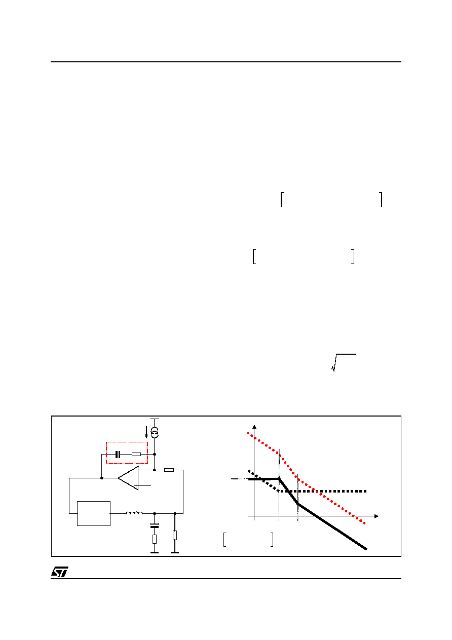
The ACM control loop gain is designed to obtain a high DC gain to minimize static error and cross the 0dB axes
with a constant -20dB/dec slope with the desired crossover frequency
ωT. Neglecting the effect of ZF(s), the
transfer function has one zero and two poles. Both the poles are fixed once the output filter is designed and the
zero is fixed by ESR and the Droop resistance. To obtain the desired shape an RF-CF series network is consid-
ered for the ZF(s) implementation. A zero at ωF=1/RFCF is then introduced together with an integrator. This in-
tegrator minimizes the static error while placing the zero in correspondence with the L-C resonance a simple -
20dB/dec shape of the gain is assured (See Figure 14). In fact, considering the usual value for the output filter,
the LC resonance results to be at frequency lower than the above reported zero.Compensation network can be
simply designed placing
ωZ = ωLC and imposing the cross-over frequency ωT as desired obtaining:
Figure 14. ACM Control Loop Gain Block Diagram (left) and Bode Diagram (right)
PWM
4
5
---
V
IN
V
OSC
-------------------
=
G
LOOP s
()
4
5
---
V
IN
V
OS C
-------------------
Z
F s
()
Z
P s
() Z
L s
()
+
------------------------------------
Rs
Rg
--------
Z
P s
()
R
FB
---------------
+
–
=
G
LOO P s
()
4
5
---
V
IN
V
OSC
-------------------
Z
F s
()
R
FB
---------------
Ro
R
DROOP
+
Ro
R
L
2
-------
+
--------------------------------------
1s Co
R
DROOP//Ro
ESR
+
()
+
s
2
Co
L
2
---
s
L
2R o
---------------
Co ESR
Co
R
L
2
-------
+
+
1
+
+
----------------------------------------------------------------------------------------------------------------------------------
–
=
G
LOO P s
()
4
5
---
V
IN
V
OSC
-------------------
Z
F s
()
R
FB
---------------
1s Co
R
DROOP
ESR
+
()
+
s
2
Co
L
2
---
s
L
2Ro
---------------
Co ESR
Co
R
L
2
-------
+
+
1
+
+
----------------------------------------------------------------------------------------------------------------------------------
–
=
R
F
R
FB
V
OSC
V
IN
----------------------------------
5
4
---
ω
T
L
2R
DROOP
ESR
+
()
--------------------------------------------------------
=
C
F
Co
L
2
---
R
F
--------------------
=
Rout
Cout
ESR
L/2
RFB
RF
CF
REF
PWM
IFB
VCOMP
VOUT
d
VIN
ZF
dB
ω
T
ω
Z
ω
LC
GLOOP
ZF(s)
K
4
5
---
V
IN
V
osc
---------------
1
R
FB
----------
dB
=
相关PDF资料 |
PDF描述 |
|---|---|
| L6919E | SWITCHING CONTROLLER, PDSO28 |
| L6920DTR | 1.2 A SWITCHING REGULATOR, PDSO8 |
| L6920D | 1.2 A SWITCHING REGULATOR, PDSO8 |
| L6920 | 1.2 A SWITCHING REGULATOR, PDSO8 |
| L6924D013TR | 1-CHANNEL POWER SUPPLY SUPPORT CKT, QCC16 |
相关代理商/技术参数 |
参数描述 |
|---|---|
| L6919CDTR | 功能描述:DC/DC 开关控制器 Prog Dual-Phase Cont RoHS:否 制造商:Texas Instruments 输入电压:6 V to 100 V 开关频率: 输出电压:1.215 V to 80 V 输出电流:3.5 A 输出端数量:1 最大工作温度:+ 125 C 安装风格: 封装 / 箱体:CPAK |
| L6919E | 功能描述:DC/DC 开关控制器 5-Bit Dual Ph Contlr RoHS:否 制造商:Texas Instruments 输入电压:6 V to 100 V 开关频率: 输出电压:1.215 V to 80 V 输出电流:3.5 A 输出端数量:1 最大工作温度:+ 125 C 安装风格: 封装 / 箱体:CPAK |
| L6919ETR | 功能描述:DC/DC 开关控制器 5-Bit Dual Ph Contlr RoHS:否 制造商:Texas Instruments 输入电压:6 V to 100 V 开关频率: 输出电压:1.215 V to 80 V 输出电流:3.5 A 输出端数量:1 最大工作温度:+ 125 C 安装风格: 封装 / 箱体:CPAK |
| L-692 | 制造商:RHOMBUS-IND 制造商全称:Rhombus Industries Inc. 功能描述:Common Mode Inductor |
| L6920 | 制造商:STMICROELECTRONICS 制造商全称:STMicroelectronics 功能描述:1V HIGH EFFICIENCY SYNCRONOUS STEP UP CONVERTER |
发布紧急采购,3分钟左右您将得到回复。