- 您现在的位置:买卖IC网 > PDF目录43901 > L6919CD (STMICROELECTRONICS) SWITCHING CONTROLLER, 200 kHz SWITCHING FREQ-MAX, PDSO28 PDF资料下载
参数资料
| 型号: | L6919CD |
| 厂商: | STMICROELECTRONICS |
| 元件分类: | 稳压器 |
| 英文描述: | SWITCHING CONTROLLER, 200 kHz SWITCHING FREQ-MAX, PDSO28 |
| 封装: | SO-28 |
| 文件页数: | 3/32页 |
| 文件大小: | 558K |
| 代理商: | L6919CD |
第1页第2页当前第3页第4页第5页第6页第7页第8页第9页第10页第11页第12页第13页第14页第15页第16页第17页第18页第19页第20页第21页第22页第23页第24页第25页第26页第27页第28页第29页第30页第31页第32页
11/32
L6919C
The BOOTx and VCCDR pins are separated from IC's power supply (VCC pin) as well as signal ground (SGND
pin) and power ground (PGND pin) in order to maximize the switching noise immunity. The separated supply
for the different drivers gives high flexibility in mosfet choice, allowing the use of logic-level mosfet. Several com-
bination of supply can be chosen to optimize performance and efficiency of the application. Power conversion
is also flexible; 5V or 12V bus can be chosen freely.
The peak current is shown for both the upper and the lower driver of the two phases in figure 3. A 10nF capac-
itive load has been used. For the upper drivers, the source current is 1.9A while the sink current is 1.5A with
VBOOT -VPHASE = 12V; similarly, for the lower drivers, the source current is 2.4A while the sink current is 2A with
VCCDR = 12V.
CURRENT READING AND OVER CURRENT
The current flowing trough each phase is read using the voltage drop across the low side mosfets RdsON or
across a sense resistor (RSENSE) and internally converted into a current. The Tran conductance ratio is issued
by the external resistor Rg placed outside the chip between ISENx and PGNDSx pins toward the reading points.
The full differential current reading rejects noise and allows to place sensing element in different locations with-
out affecting the measurement's accuracy. The current reading circuitry reads the current during the time in
which the low-side mosfet is on (OFF Time). During this time, the reaction keeps the pin ISENx and PGNDSx
at the same voltage while during the time in which the reading circuitry is off, an internal clamp keeps these two
pins at the same voltage sinking from the ISENx pin the necessary current (Needed if low-side mosfet RdsON
sense is implemented to avoid absolute maximum rating overcome on ISENx pin).
The proprietary current reading circuit allows a very precise and high bandwidth reading for both positive and
negative current. This circuit reproduces the current flowing through the sensing element using a high speed
Track & Hold Tran conductance amplifier. In particular, it reads the current during the second half of the OFF
time reducing noise injection into the device due to the mosfet turn-on (See fig. 5). Track time must be at least
200ns to make proper reading of the delivered current
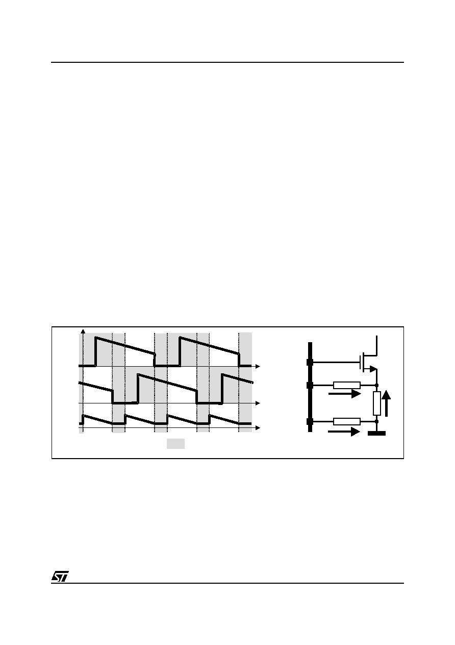
Figure 5. Current Reading Timing (Left) and Circuit (Right)
This circuit sources a constant 50
A current from the PGNDSx pin and keeps the pins ISENx and PGNDSx at
the same voltage. Referring to figure 4, the current that flows in the ISENx pin is then given by the following
equation:
Where RSENSE is an external sense resistor or the rds,on of the low side mosfet and Rg is the transconductance
resistor used between ISENx and PGNDSx pins toward the reading points; IPHASE is the current carried by each
phase and, in particular, the current measured in the middle of the oscillator period
The current information reproduced internally is represented by the second term of the previous equation as
R
SE
NSE
Rg
50
A
IISENx
I
P
H
AS
E
Rg
LGATEX
ISENX
PGNDSX
ILS1
ILS2
Track & Hold
Total current
information
I
ISENx
50
A
R
SENSE
I
PHASE
R
g
----------------------------------------------
+
50
AI
IN FO x
+
==
相关PDF资料 |
PDF描述 |
|---|---|
| L6919E | SWITCHING CONTROLLER, PDSO28 |
| L6920DTR | 1.2 A SWITCHING REGULATOR, PDSO8 |
| L6920D | 1.2 A SWITCHING REGULATOR, PDSO8 |
| L6920 | 1.2 A SWITCHING REGULATOR, PDSO8 |
| L6924D013TR | 1-CHANNEL POWER SUPPLY SUPPORT CKT, QCC16 |
相关代理商/技术参数 |
参数描述 |
|---|---|
| L6919CDTR | 功能描述:DC/DC 开关控制器 Prog Dual-Phase Cont RoHS:否 制造商:Texas Instruments 输入电压:6 V to 100 V 开关频率: 输出电压:1.215 V to 80 V 输出电流:3.5 A 输出端数量:1 最大工作温度:+ 125 C 安装风格: 封装 / 箱体:CPAK |
| L6919E | 功能描述:DC/DC 开关控制器 5-Bit Dual Ph Contlr RoHS:否 制造商:Texas Instruments 输入电压:6 V to 100 V 开关频率: 输出电压:1.215 V to 80 V 输出电流:3.5 A 输出端数量:1 最大工作温度:+ 125 C 安装风格: 封装 / 箱体:CPAK |
| L6919ETR | 功能描述:DC/DC 开关控制器 5-Bit Dual Ph Contlr RoHS:否 制造商:Texas Instruments 输入电压:6 V to 100 V 开关频率: 输出电压:1.215 V to 80 V 输出电流:3.5 A 输出端数量:1 最大工作温度:+ 125 C 安装风格: 封装 / 箱体:CPAK |
| L-692 | 制造商:RHOMBUS-IND 制造商全称:Rhombus Industries Inc. 功能描述:Common Mode Inductor |
| L6920 | 制造商:STMICROELECTRONICS 制造商全称:STMicroelectronics 功能描述:1V HIGH EFFICIENCY SYNCRONOUS STEP UP CONVERTER |
发布紧急采购,3分钟左右您将得到回复。