- 您现在的位置:买卖IC网 > PDF目录30719 > LA4815M (SANYO SEMICONDUCTOR CO LTD) 0.62 W, 1 CHANNEL, AUDIO AMPLIFIER, PDSO8 PDF资料下载
参数资料
| 型号: | LA4815M |
| 厂商: | SANYO SEMICONDUCTOR CO LTD |
| 元件分类: | 音频/视频放大 |
| 英文描述: | 0.62 W, 1 CHANNEL, AUDIO AMPLIFIER, PDSO8 |
| 封装: | 0.225 INCH, MFP-8 |
| 文件页数: | 11/14页 |
| 文件大小: | 233K |
| 代理商: | LA4815M |
LA4815M
Notes on Using the IC
1. Voltage gain settings (Pins 1 and 8)
The voltage gain of the power amplifier is fixed by the internal resistors.
Pins 1 and 8 be left open : Approximately 26dB
Pins 1 and 8 connected to GND : Approximately 39.5dB
Note that the voltage gain can be changed using two resistors. (See Fig. 1)
Voltage gain setting : According to the resistor connected between Pin 8 and Pin 2 (GND1)
* Voltage gain = 20log (20
× (625 + Rvg1)/(125 + Rvg1))
Output DC voltage setting : According to the resistor connected between Pin 1 and Pin 2 (GND1)
* Rvg1 = Rvg2 must be satisfied.
In addition, the voltage gain can also be lowered to approximately 20dB (when using 5V or 6V power supply) by an
application such as shown in Fig. 2 below.
Voltage gain setting : According to the resistor connected between Pin 8 and Pin 5 (OUT)
* Voltage gain = 20log (20
× (125 + Rvg3)/(10,125 + Rvg3))
Output DC voltage setting : According to the resistor connected between Pin 1 and Pin 6 (VCC)
* Set the resistor values so that the Pin 5 (OUT) DC voltage is approximately half the supply voltage.
Example : When Rvg3 = 10k
Ω, Rvg4 = 22kΩ (when VCC = 6V)
However, note that using this method to greatly lower the voltage gain deteriorates the characteristics, so the voltage
gain should be lowered only to approximately 20dB. In addition, when using a high supply voltage (7V or more), the
clipped waveform may invert, so this voltage gain reduction method must not be used in these cases.
LA4815M
Rvg1
Rvg2
GAIN2
GAIN1
GND1
VCC
OUT
LA4815M
Rvg3
Rvg4
GAIN2
GAIN1
GND1
VCC
OUT
1
2
3
4
8
7
6
5
1
2
3
4
8
7
6
5
Figure 1
Figure 2
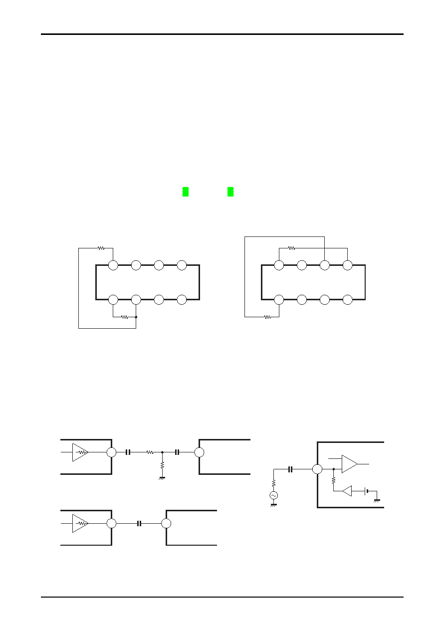
2. Signal source impedance : rg
The signal source impedance value rg affects the ripple rejection ratio together with input coupling capacitor Cin, so rg
should be as small as possible. Therefore, when attenuating the signal at the Cin front end as shown in Fig. 4, the
constants should be set in consideration of these characteristics. Using the smallest resistor Rg1 value possible is
recommended.
In addition, when setting the signal level, the voltage gain should be set on the LA4815M side and the input front-end
should be configured using only the input coupling capacitor, Cin, as shown in Fig. 5 in order to maximize the ripple
rejection ratio.
Vbias
100k
Ω
+
-
Pre-Amp
Rg2
Cin
Rg1
rg
OUT
other IC
ro
LA4815M
IN
Cin
other IC
ro
LA4815M
Cin
IN
3
OUT
IN
3
Figure 4
Figure 3
Figure 5
No.A1373-6/14
相关PDF资料 |
PDF描述 |
|---|---|
| LA4815 | 5 W, 2 CHANNEL, AUDIO AMPLIFIER, DIP28 |
| LA4815 | 5 W, 2 CHANNEL, AUDIO AMPLIFIER, DIP28 |
| LA4820M | 0.12 W, 2 CHANNEL, AUDIO AMPLIFIER, PDSO24 |
| LA4901 | 10 W, 1 CHANNEL, AUDIO AMPLIFIER, DIP28 |
| LA4902 | 10 W, 1 CHANNEL, AUDIO AMPLIFIER, DIP28 |
相关代理商/技术参数 |
参数描述 |
|---|---|
| LA4815M_10 | 制造商:SANYO 制造商全称:Sanyo Semicon Device 功能描述:Monaural Power Amplifier |
| LA4815M-TLM-H | 功能描述:功率放大器 MONAURAL POWER AMPLIFIER RoHS:否 制造商:TriQuint Semiconductor 封装 / 箱体: 工作电源电压:28 V 电源电流:2.5 A 工作温度范围: 封装: |
| LA4815VH | 制造商:SANYO 制造商全称:Sanyo Semicon Device 功能描述:Monaural Power Amplifier |
| LA4815VH_12 | 制造商:SANYO 制造商全称:Sanyo Semicon Device 功能描述:Monaural Power Amplifier |
| LA4815VH-MPB-H | 功能描述:音频放大器 RoHS:否 制造商:STMicroelectronics 产品:General Purpose Audio Amplifiers 输出类型:Digital 输出功率: THD + 噪声: 工作电源电压:3.3 V 电源电流: 最大功率耗散: 最大工作温度: 安装风格:SMD/SMT 封装 / 箱体:TQFP-64 封装:Reel |
发布紧急采购,3分钟左右您将得到回复。