- 您现在的位置:买卖IC网 > PDF目录30721 > LA72700V SPECIALTY CONSUMER CIRCUIT, PDSO36 PDF资料下载
参数资料
| 型号: | LA72700V |
| 元件分类: | 消费家电 |
| 英文描述: | SPECIALTY CONSUMER CIRCUIT, PDSO36 |
| 封装: | 0.275 INCH, SSOP-36 |
| 文件页数: | 6/16页 |
| 文件大小: | 517K |
| 代理商: | LA72700V |
LC72710W, 72710LW
No.6166-14/30
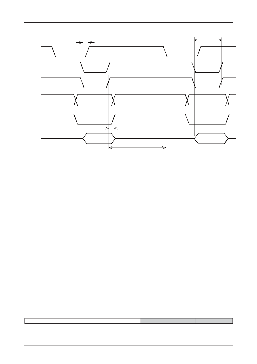
Post-Correction Data Read Timing (DMA)
Layer 4 CRC Detection Circuit <Parallel Interface>
This function provides data group error detection, i.e. layer 4 CRC. When the stipulated number of bytes of data group
data and the CRC detection word (16 bits) are written to the layer 4 CRC register (address 6), if either the CRC4 pin
outputs a high level or the CRC4 flag (bit 1 in the status register at address 1) is set to 1 then there were no errors in the
data. The CRC4 pin or CRC4 flag in the status register outputs a high level if the IC internal CRC detection register bits
are all in the logic 0 state.
When this function is used to perform a layer 4 CRC check, applications must initialize the IC internal CRC detection
register before transferring the data for a single data group. This initialization is performed by sending data for bit 7
(CRC4_RST) in control register 1. Note that since this initialization flag is not automatically reset to 0, after the
application sets this flag it must then send another data item that resets it to 0 before sending the layer 4 CRC check
data.
If there were no errors in all the received data groups, the CRC register will, necessarily, be all zeros after the CRC
check for a given data group. Therefore, as long as there are no errors detected in the layer 4 CRC check, the application
does not need to initialize the CRC detection register again using the control register as described above. There is no
upper limit on the total data length of data groups that can be transferred. Also, when the serial interface issued, the
CCB transfers can be divided into multiple transfer operations. The generating polynomial G(x) for the CRC code is as
follows. G (x) = X16 + X12 + X5 + 1
Structure of the Post-Correction Output Data <Parallel Interface>
The total length of the prepared output data is always 176 bits, i.e. 22 bytes. The layer 2 CRC data (14 bits) and the
parity data (82 bits) are not output. The data in each packet in the post-correction data is output in order starting at the
beginning in 8- or 16-bit units. BIC codes are not output.
When the CPU reads out the data, it can easily select the data by checking the status register first. The CPU can then
simply ignore data determined to be unnecessary without having to read it out by simply waiting until the next interrupt
arrives.
Data block (176bits) Post-error correction data
Layer 2 CRC (14bits)
Parity (82bits)
*: This data is not output.
Structure of a Single Data Packet (Total length: 272bits. BIC is not included.)
CS
RD
A0 to A3
DATn
DACK
DREQ
tDREQ
tRDH
tCYDM
tWRDM
*: A0 to A3: When post-correction data is read, A0 to A3 will be held fixed at 0.
*: DREQ and DACK: The polarity of these signals can be set.
*: Applications can select whether the DR or DACK signal is used for readout.
相关PDF资料 |
PDF描述 |
|---|---|
| LA72700V | SPECIALTY CONSUMER CIRCUIT, PDSO36 |
| LA72702NV | SPECIALTY CONSUMER CIRCUIT, PDSO24 |
| LA72702NV | SPECIALTY CONSUMER CIRCUIT, PDSO24 |
| LA72702VA | SPECIALTY CONSUMER CIRCUIT, PDSO24 |
| LA7270 | 2 CHANNEL, VIDEO PREAMPLIFIER, PDIP22 |
相关代理商/技术参数 |
参数描述 |
|---|---|
| LA72700V-MPB-E | 制造商:ON Semiconductor 功能描述:VIDEO ICS - Ammo Pack |
| LA72700V-N-MPB-E | 制造商:ON Semiconductor 功能描述:VIDEO ICS - Ammo Pack |
| LA72700V-N-TLM-E | 制造商:ON Semiconductor 功能描述:VIDEO ICS - Tape and Reel 制造商:ON Semiconductor 功能描述:REEL / VIDEO ICS |
| LA72702NV | 制造商:SANYO 制造商全称:Sanyo Semicon Device 功能描述:Monolithic Linear IC For US TV BTSC Decoder |
| LA72702NV-MPB-E | 功能描述:编码器、解码器、复用器和解复用器 RoHS:否 制造商:Micrel 产品:Multiplexers 逻辑系列:CMOS 位数: 线路数量(输入/输出):2 / 12 传播延迟时间:350 ps, 400 ps 电源电压-最大:2.625 V, 3.6 V 电源电压-最小:2.375 V, 3 V 最大工作温度:+ 85 C 安装风格:SMD/SMT 封装 / 箱体:QFN-44 封装:Tray |
发布紧急采购,3分钟左右您将得到回复。