- 您现在的位置:买卖IC网 > PDF目录67755 > LB1693 BRUSHLESS DC MOTOR CONTROLLER, 2.5 A, PDIP20 PDF资料下载
参数资料
| 型号: | LB1693 |
| 元件分类: | 运动控制电子 |
| 英文描述: | BRUSHLESS DC MOTOR CONTROLLER, 2.5 A, PDIP20 |
| 封装: | 0.500 INCH, DIP-20 |
| 文件页数: | 11/11页 |
| 文件大小: | 159K |
| 代理商: | LB1693 |
LB1693
No.3295-9/11
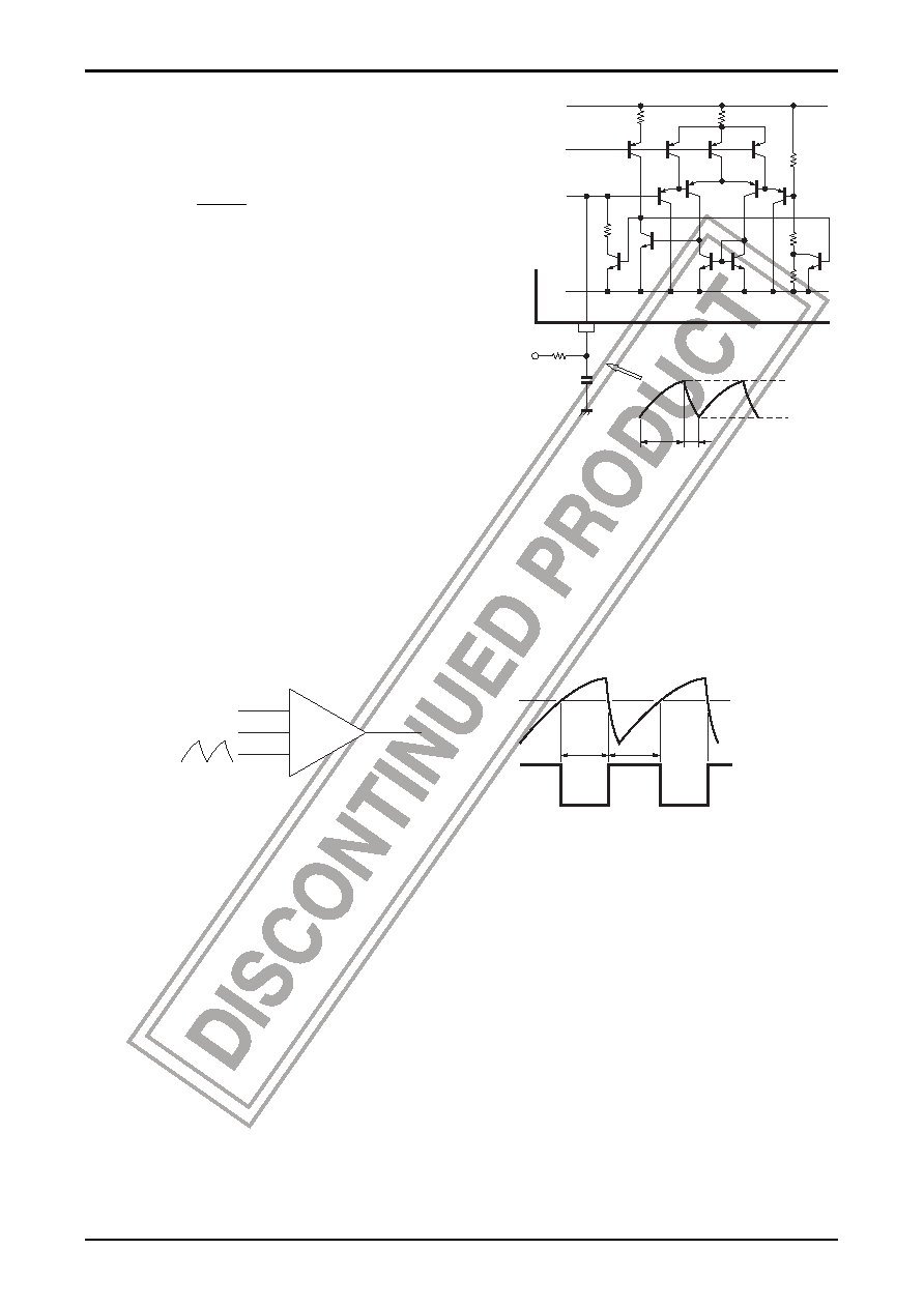
1. Switching regulator oscillation circuit (PWM generation circuit)
1-1. Oscillation circuit (40 to 50kHz max.)
Figure 1 shows the oscillation circuit that generates the
triangular waves. The oscillation frequency for this circuit
is detemined by the following equation (with VH = 7V typ.)
f =
1
t0 + t1
(Hz)
t0 ≈ 0.56CR (charging)
t1 ≈ 1.34CRN (discharging)
(RN is the internal resistance of 1.4kΩ approx.)
In actual applications, R
>> RN is used to suppress the influence
of variation in the IC’s internal resistance.
Figure 1 Oscillation Circuit
1-2. Comparator circuit
Figure 2 shows the comparator circuit for comparing the triangular
wave output, the speed control signal, etc.
input terminals
CR
Input the triangular wave output.
VCONT
Input the speed control signal.
C
Goes high when current limiter 2 is operating.
(When VC(H) > VCR(H), the OSC output is off.)
Figure 2. Comparator Circuit
2. Position detection circuit (Hall element input circuit)
The position detection circuit is a differential amp with hysteresis (38mV typ.). For the operating DC level, use within
the common-mode phase input voltage range (1.5 to VH-1.8V). Also it is recommended that the input level is at least
three times (150 to 200mVp-p) the hysteresis.
3. VH power supply circuit
The VH power supply pins can be used to from the internal power supply or an external power supply.
When using the internal power supply, the internal logic operates with VH = 7V typical (VCC = 24V). When using an
external power supply, set VCC = VH = 5V and operate the internal logic at 5V.
C
+
-
VCONT
OSC
CR
VCR
VCONT
OSC
OFF
ON
OFF
ON
tON
tOFF
CR
VCR(H)
VCR(L)
VH
R
RN
C
t0
t1
VCR
相关PDF资料 |
PDF描述 |
|---|---|
| LB1823 | BRUSHLESS DC MOTOR CONTROLLER, 0.03 A, PDIP30 |
| LB1889M | BRUSHLESS DC MOTOR CONTROLLER, 1.3 A, PDSO36 |
| LB1889D | BRUSHLESS DC MOTOR CONTROLLER, 1.3 A, PDIP28 |
| LB1923M | BRUSHLESS DC MOTOR CONTROLLER, 0.03 A, PQFP44 |
| LB1946 | STEPPER MOTOR CONTROLLER, 1.75 A, PDFM28 |
相关代理商/技术参数 |
参数描述 |
|---|---|
| LB1694N | 制造商:SANYO 制造商全称:Sanyo Semicon Device 功能描述:3-Phase Brushless Motor Driver |
| LB1694N-E | 制造商:ON Semiconductor 功能描述:3PHASE MOTOR DRIVER - Ammo Pack |
| LB1695 | 制造商:SANYO 制造商全称:Sanyo Semicon Device 功能描述:Three-Phase Brushless Motor Driver |
| LB1695D | 制造商:SANYO 制造商全称:Sanyo Semicon Device 功能描述:LB1695D |
| LB1695M | 制造商:SANYO 制造商全称:Sanyo Semicon Device 功能描述:DC Fan Motor Driver |
发布紧急采购,3分钟左右您将得到回复。