- 您现在的位置:买卖IC网 > PDF目录67755 > LB1693 BRUSHLESS DC MOTOR CONTROLLER, 2.5 A, PDIP20 PDF资料下载
参数资料
| 型号: | LB1693 |
| 元件分类: | 运动控制电子 |
| 英文描述: | BRUSHLESS DC MOTOR CONTROLLER, 2.5 A, PDIP20 |
| 封装: | 0.500 INCH, DIP-20 |
| 文件页数: | 6/11页 |
| 文件大小: | 159K |
| 代理商: | LB1693 |
LB1693
No.3295-4/11
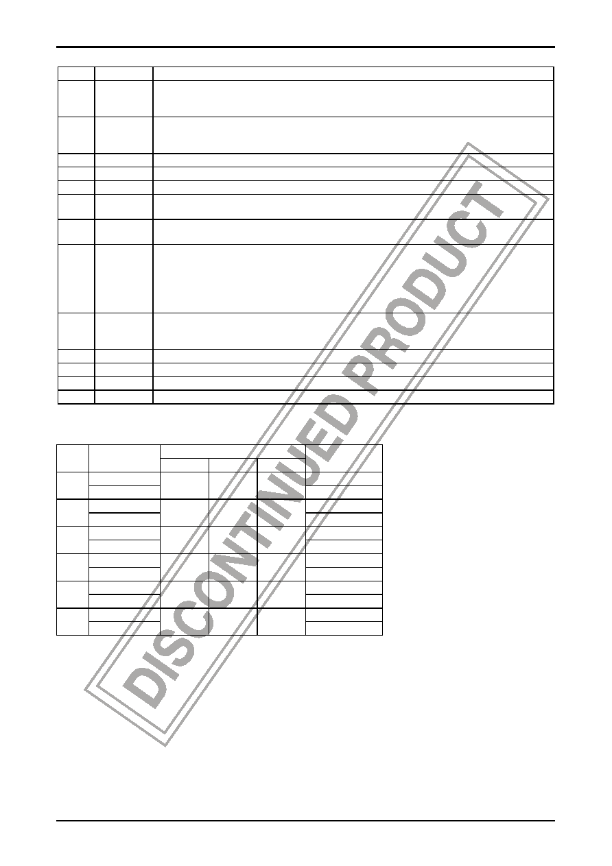
Pin Functions
Pin No.
Pin name
Function
17, 18
15, 16
13, 14
IN1+, IN1-
IN2+, IN2-
IN3+, IN3-
OUT1 : Hall element input pins for Phase 1. High logic is the state when IN+ > IN-.
OUT2 : Hall element input pins for Phase 2. High logic is the state when IN+ > IN-.
OUT3 : Hall element input pins for Phase 3. High logic is the state when IN+ > IN-.
6
7
8
OUT1
OUT2
OUT3
Output pin for Phase 1.
Output pin for Phase 2.
Output pin for Phase 3.
11
VCC
Power supply pin for applying voltage to each section other than output section.
10
VM
Power supply that provides the output power.
9
RF
Output current detect pin ; RF is inserted between this pin and ground to detect the output current as a voltage.
12
GND
Ground for other output.
The minimum potential of output transistor is at the RF pin.
19
BR
Brake pin.
The brake is switched on/off by setting this pin high (2V or more)/low (0.8V or less).
20
FSR
Forward/stop/reverse control pin.
The motor is driven forward, stopped, or driven in reverse according to the voltage at this pin.
Forward : 0 to 0.8V
Stop :
2.1 to 2.9V
Reverse : 4.2 to 5.0V
5
VH
Power pin for Hall elements.
When using the internal (stabilized) power supply : VH = 7V typ.
When using the external (stabilized) power supply : VH = 5V typ.
1
CR
Sets the oscillation frequency for the switching regulator.
2
OSC
Outputs duty-controlled pulsed ; open collector output.
3
VCONT
Speed control pin ; varies the swithcing regulator output votlage.
4
C
Suppresses ripples in the motor current during operation of current limiter 2.
Truth Table
Input
Item
Source Sink
IN1
IN2
IN3
Forward/Reverse
Control FSR
OUT3→OUT2
L
1
OUT2→OUT3
H
L
H
OUT3→OUT1
L
2
OUT1→OUT3
H
L
H
OUT2→OUT3
L
3
OUT3→OUT2
L
H
OUT1→OUT2
L
4
OUT2→OUT1
L
H
L
H
OUT2→OUT1
L
5
OUT1→OUT2
H
L
H
OUT1→OUT3
L
6
OUT3→OUT1
L
H
相关PDF资料 |
PDF描述 |
|---|---|
| LB1823 | BRUSHLESS DC MOTOR CONTROLLER, 0.03 A, PDIP30 |
| LB1889M | BRUSHLESS DC MOTOR CONTROLLER, 1.3 A, PDSO36 |
| LB1889D | BRUSHLESS DC MOTOR CONTROLLER, 1.3 A, PDIP28 |
| LB1923M | BRUSHLESS DC MOTOR CONTROLLER, 0.03 A, PQFP44 |
| LB1946 | STEPPER MOTOR CONTROLLER, 1.75 A, PDFM28 |
相关代理商/技术参数 |
参数描述 |
|---|---|
| LB1694N | 制造商:SANYO 制造商全称:Sanyo Semicon Device 功能描述:3-Phase Brushless Motor Driver |
| LB1694N-E | 制造商:ON Semiconductor 功能描述:3PHASE MOTOR DRIVER - Ammo Pack |
| LB1695 | 制造商:SANYO 制造商全称:Sanyo Semicon Device 功能描述:Three-Phase Brushless Motor Driver |
| LB1695D | 制造商:SANYO 制造商全称:Sanyo Semicon Device 功能描述:LB1695D |
| LB1695M | 制造商:SANYO 制造商全称:Sanyo Semicon Device 功能描述:DC Fan Motor Driver |
发布紧急采购,3分钟左右您将得到回复。