- 您现在的位置:买卖IC网 > PDF目录177662 > LC4512B-10FN256I (LATTICE SEMICONDUCTOR CORP) PDF资料下载
参数资料
| 型号: | LC4512B-10FN256I |
| 厂商: | LATTICE SEMICONDUCTOR CORP |
| 元件分类: | PLD |
| 中文描述: | EE PLD, 10 ns, PBGA256 |
| 封装: | LEAD FREE, FPBGA-256 |
| 文件页数: | 78/99页 |
| 文件大小: | 441K |
| 代理商: | LC4512B-10FN256I |
第1页第2页第3页第4页第5页第6页第7页第8页第9页第10页第11页第12页第13页第14页第15页第16页第17页第18页第19页第20页第21页第22页第23页第24页第25页第26页第27页第28页第29页第30页第31页第32页第33页第34页第35页第36页第37页第38页第39页第40页第41页第42页第43页第44页第45页第46页第47页第48页第49页第50页第51页第52页第53页第54页第55页第56页第57页第58页第59页第60页第61页第62页第63页第64页第65页第66页第67页第68页第69页第70页第71页第72页第73页第74页第75页第76页第77页当前第78页第79页第80页第81页第82页第83页第84页第85页第86页第87页第88页第89页第90页第91页第92页第93页第94页第95页第96页第97页第98页第99页
Lattice Semiconductor
ispMACH 4000V/B/C/Z Family Data Sheet
8
Block CLK2
Block CLK3
PT Clock
PT Clock Inverted
Shared PT Clock
Ground
Clock Enable Multiplexer
Each macrocell has a 4:1 clock enable multiplexer. This allows the clock enable signal to be selected from the fol-
lowing four sources:
PT Initialization/CE
PT Initialization/CE Inverted
Shared PT Clock
Logic High
Initialization Control
The ispMACH 4000 family architecture accommodates both block-level and macrocell-level set and reset capability.
There is one block-level initialization term that is distributed to all macrocell registers in a GLB. At the macrocell
level, two product terms can be “stolen” from the cluster associated with a macrocell to be used for set/reset func-
tionality. A reset/preset swapping feature in each macrocell allows for reset and preset to be exchanged, providing
exibility.
Note that the reset/preset swapping selection feature affects power-up reset as well. All ip-ops power up to a
known state for predictable system initialization. If a macrocell is congured to SET on a signal from the block-level
initialization, then that macrocell will be SET during device power-up. If a macrocell is congured to RESET on a
signal from the block-level initialization or is not congured for set/reset, then that macrocell will RESET on power-
up. To guarantee initialization values, the VCC rise must be monotonic, and the clock must be inactive until the reset
delay time has elapsed.
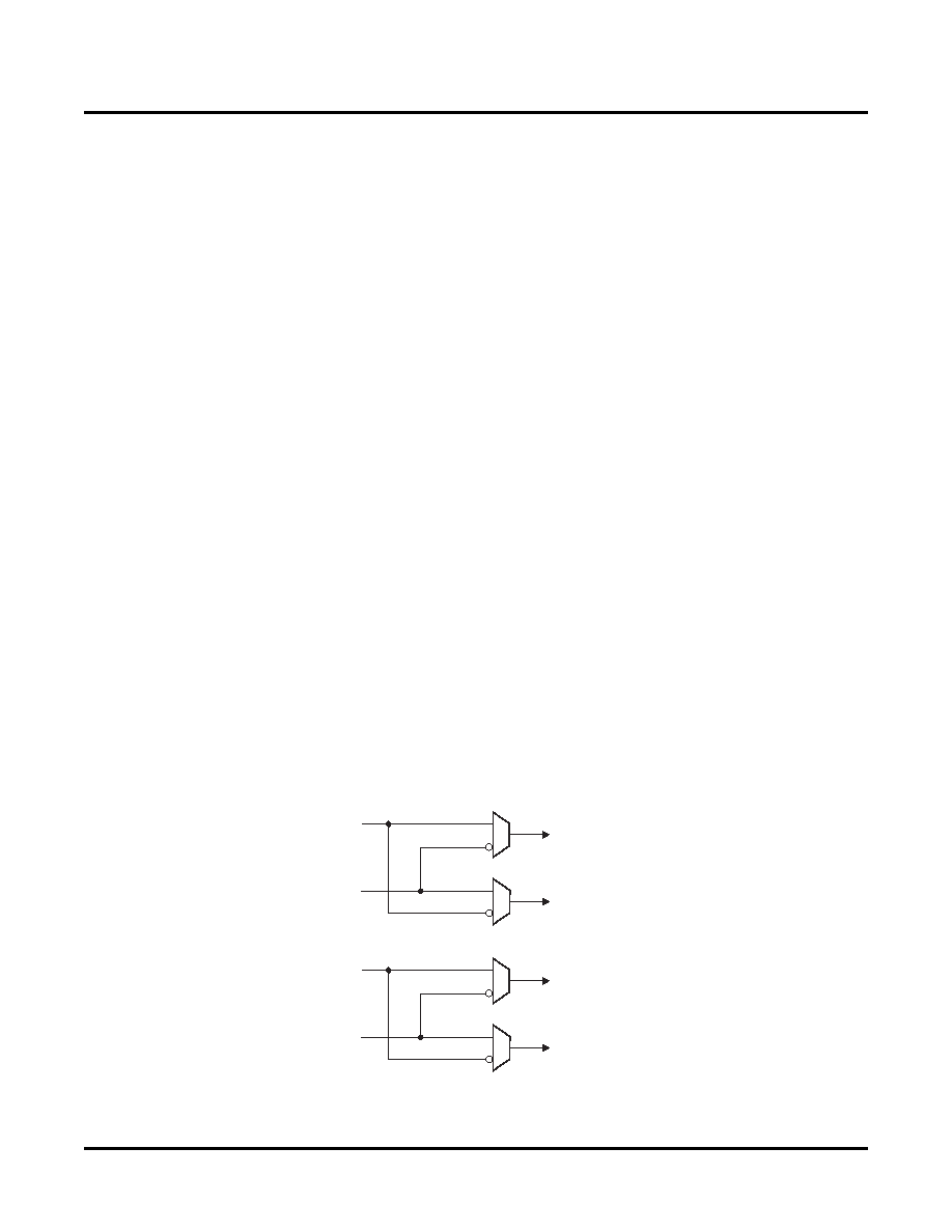
GLB Clock Generator
Each ispMACH 4000 device has up to four clock pins that are also routed to the GRP to be used as inputs. These
pins drive a clock generator in each GLB, as shown in Figure 6. The clock generator provides four clock signals that
can be used anywhere in the GLB. These four GLB clock signals can consist of a number of combinations of the
true and complement edges of the global clock signals.
Figure 6. GLB Clock Generator
CLK0
CLK1
CLK2
CLK3
Block CLK0
Block CLK1
Block CLK2
Block CLK3
相关PDF资料 |
PDF描述 |
|---|---|
| LC4384C-5FN256I | |
| LC4512B-35FN256C | |
| LC4256B-5FN256BC | |
| LC4256C-5FN256BC | |
| LC4256B-10FN256BI | |
相关代理商/技术参数 |
参数描述 |
|---|---|
| LC4512B-10FN256I1 | 制造商:LATTICE 制造商全称:Lattice Semiconductor 功能描述:3.3V/2.5V/1.8V In-System Programmable SuperFAST High Density PLDs |
| LC4512B-10FT256I | 功能描述:CPLD - 复杂可编程逻辑器件 ispJTAG 2.5V 10nsIND 512MC 208 I/O RoHS:否 制造商:Lattice 系列: 存储类型:EEPROM 大电池数量:128 最大工作频率:333 MHz 延迟时间:2.7 ns 可编程输入/输出端数量:64 工作电源电压:3.3 V 最大工作温度:+ 90 C 最小工作温度:0 C 封装 / 箱体:TQFP-100 |
| LC4512B-10FTN256I | 功能描述:CPLD - 复杂可编程逻辑器件 ispJTAG 2.5V 10nsIND 512MC 208 I/O RoHS:否 制造商:Lattice 系列: 存储类型:EEPROM 大电池数量:128 最大工作频率:333 MHz 延迟时间:2.7 ns 可编程输入/输出端数量:64 工作电源电压:3.3 V 最大工作温度:+ 90 C 最小工作温度:0 C 封装 / 箱体:TQFP-100 |
| LC4512B-10T176I | 功能描述:CPLD - 复杂可编程逻辑器件 PROGRAMMABLE SUPER FAST HI DENSITY PLD RoHS:否 制造商:Lattice 系列: 存储类型:EEPROM 大电池数量:128 最大工作频率:333 MHz 延迟时间:2.7 ns 可编程输入/输出端数量:64 工作电源电压:3.3 V 最大工作温度:+ 90 C 最小工作温度:0 C 封装 / 箱体:TQFP-100 |
| LC4512B-10TN176I | 功能描述:CPLD - 复杂可编程逻辑器件 PROGRAMMABLE SUPER FAST HI DENSITY PLD RoHS:否 制造商:Lattice 系列: 存储类型:EEPROM 大电池数量:128 最大工作频率:333 MHz 延迟时间:2.7 ns 可编程输入/输出端数量:64 工作电源电压:3.3 V 最大工作温度:+ 90 C 最小工作温度:0 C 封装 / 箱体:TQFP-100 |
发布紧急采购,3分钟左右您将得到回复。