- 您现在的位置:买卖IC网 > PDF目录177666 > LC51024MC-52F672C (LATTICE SEMICONDUCTOR CORP) PDF资料下载
参数资料
| 型号: | LC51024MC-52F672C |
| 厂商: | LATTICE SEMICONDUCTOR CORP |
| 元件分类: | PLD |
| 中文描述: | EE PLD, 6.5 ns, PBGA672 |
| 封装: | FPBGA-672 |
| 文件页数: | 3/95页 |
| 文件大小: | 923K |
| 代理商: | LC51024MC-52F672C |
第1页第2页当前第3页第4页第5页第6页第7页第8页第9页第10页第11页第12页第13页第14页第15页第16页第17页第18页第19页第20页第21页第22页第23页第24页第25页第26页第27页第28页第29页第30页第31页第32页第33页第34页第35页第36页第37页第38页第39页第40页第41页第42页第43页第44页第45页第46页第47页第48页第49页第50页第51页第52页第53页第54页第55页第56页第57页第58页第59页第60页第61页第62页第63页第64页第65页第66页第67页第68页第69页第70页第71页第72页第73页第74页第75页第76页第77页第78页第79页第80页第81页第82页第83页第84页第85页第86页第87页第88页第89页第90页第91页第92页第93页第94页第95页
Lattice Semiconductor
ispXPLD 5000MX Family Data Sheet
11
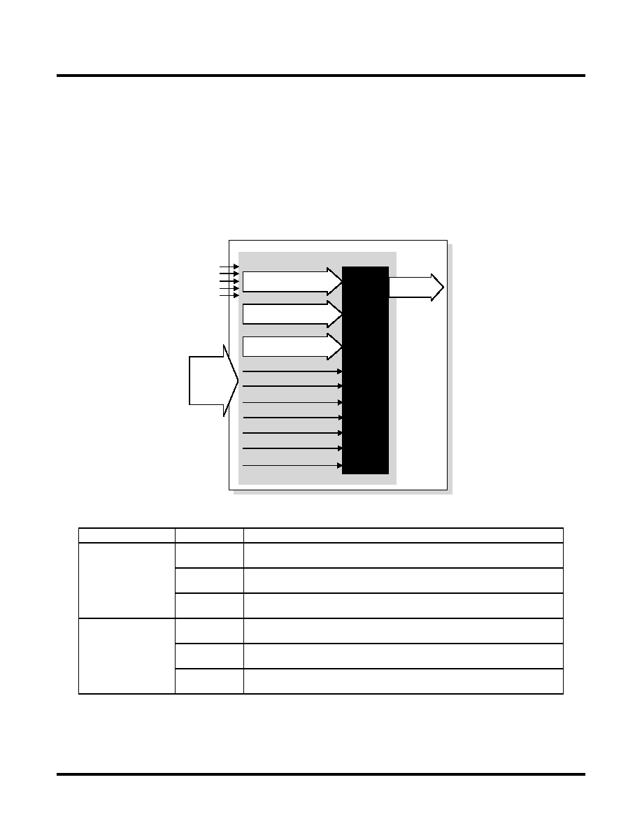
Pseudo Dual-Port SRAM Mode
In Pseudo Dual-Port SRAM Mode the multi-function array is configured as a SRAM with an independent read and
write ports that access the same 16,384-bits of memory. Data widths of 1, 2, 4, 8, 16 and 32 are supported by the
MFB. Figure 10 shows the block diagram of the Pseudo Dual-Port SRAM.
Write data, write address, chip select and write enable signals are always synchronous (registered). The read data
and read address signals can be synchronous or asynchronous. Reset is asynchronous. All write signals share the
same clock, and clock enable. All read signals share the same clock and clock enable. Reset is shared by both
read and write signals. Table 6 shows the possible sources for the clock, clock enable and initialization signals for
the various registers.
Figure 10. Pseudo Dual-Port SRAM Block Diagram
Table 6. Register Clock, Clock Enable, and Reset in Pseudo Dual-Port SRAM Mode
Register
Input
Source
Write Address, Write
Data, Write Enable,
and Write Chip Select
Clock
WCLK or one of the global clocks (CLK0 - CLK3). The selected signal can
be inverted if desired.
Clock Enable
WCEN or one of the global clocks (CLK1 - CLK2). The selected signal can
be inverted if desired.
Reset
Created by the logical OR of the global reset signal and RST. RST may have
inversion if desired.
Read Data and Read
Address
Clock
RCLK or one of the global clocks (CLK0 - CLK3). The selected signal can be
inverted if desired.
Clock Enable
RCEN or one of the global clocks (CLK1 - CLK2). The selected signal can
be inverted if desired.
Reset
Created by the logical OR of the global reset signal and RST. RST may have
inversion if desired.
‘
68 Inputs
From
Routing
16,384 bit
Pseudo
Dual
Port
SRAM
Array
Write Address
(WAD[0:8-13])
Write Clk Enable (WCEN)
Write Clock (WCLK)
Read Address
(RAD[0:8-13])
Write Enable (WE)
Write Chip Sel (WCS[0,1])
Reset (RST)
Read Clk Enable (RCEN)
Read Clock (RCLK)
Write Data
(WD[0:0,1,3,7,15,31])
RESET
CLK0
CLK3
CLK1
CLK2
Read Data
(RD[0:0-15])
相关PDF资料 |
PDF描述 |
|---|---|
| LC51024MB-75F672I | |
| LC6554H | 4-BIT, MROM, 4.33 MHz, MICROCONTROLLER, PDIP64 |
| LC864508 | 8-BIT, MROM, 12.24 MHz, MICROCONTROLLER, PDIP52 |
| LC868016A | 8-BIT, MROM, 12.24 MHz, MICROCONTROLLER, UUC138 |
| LC876596B | 8-BIT, MROM, 10 MHz, MICROCONTROLLER, PQFP100 |
相关代理商/技术参数 |
参数描述 |
|---|---|
| LC51024MC-52F672I | 制造商:LATTICE 制造商全称:Lattice Semiconductor 功能描述:3.3V, 2.5V and 1.8V In-System Programmable eXpanded Programmable Logic Device XPLD⑩ Family |
| LC51024MC-52FN208C | 制造商:LATTICE 制造商全称:Lattice Semiconductor 功能描述:3.3V, 2.5V and 1.8V In-System Programmable eXpanded Programmable Logic Device XPLD⑩ Family |
| LC51024MC-52FN208I | 制造商:LATTICE 制造商全称:Lattice Semiconductor 功能描述:3.3V, 2.5V and 1.8V In-System Programmable eXpanded Programmable Logic Device XPLD⑩ Family |
| LC51024MC-52FN256C | 制造商:LATTICE 制造商全称:Lattice Semiconductor 功能描述:3.3V, 2.5V and 1.8V In-System Programmable eXpanded Programmable Logic Device XPLD⑩ Family |
| LC51024MC-52FN256I | 制造商:LATTICE 制造商全称:Lattice Semiconductor 功能描述:3.3V, 2.5V and 1.8V In-System Programmable eXpanded Programmable Logic Device XPLD⑩ Family |
发布紧急采购,3分钟左右您将得到回复。