- 您现在的位置:买卖IC网 > PDF目录67755 > LC5521D 2.5 A POWER FACTOR CONTROLLER, 18 kHz SWITCHING FREQ-MAX, DIP7 PDF资料下载
参数资料
| 型号: | LC5521D |
| 元件分类: | 稳压器 |
| 英文描述: | 2.5 A POWER FACTOR CONTROLLER, 18 kHz SWITCHING FREQ-MAX, DIP7 |
| 封装: | DIP-8/7 |
| 文件页数: | 11/40页 |
| 文件大小: | 888K |
| 代理商: | LC5521D |
第1页第2页第3页第4页第5页第6页第7页第8页第9页第10页当前第11页第12页第13页第14页第15页第16页第17页第18页第19页第20页第21页第22页第23页第24页第25页第26页第27页第28页第29页第30页第31页第32页第33页第34页第35页第36页第37页第38页第39页第40页
19
Allegro MicroSystems, Inc.
115 Northeast Cutoff
Worcester, Massachusetts 01615-0036 U.S.A.
1.508.853.5000; www.allegromicro.com
28106.02
Figure 17. Averaged input current waveform, LC552xD and LC552xF series
FB pin voltage
S/GND
EIN
Drain current
Averaged input current
D/ST
VCC
S/GND
D
V
P
C2
2(4)
8(1)
C4
1(2)
D
L2
LC55xxD
(LC552xF)
D5
R1
VCC
= 3.7mA
ICC(ON) (max)
Sto
p
St
ar
tu
p
ICC
9.4 V
VCC(OFF)
VCC(ON)
15.1 V
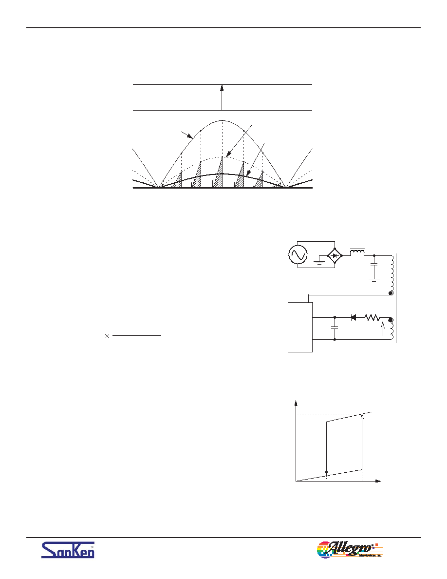
Figure 18. VCC pin peripheral circuit
Figure 19. VCC versus operation current, ICC
Startup Operation
Figure 18 shows the VCC pin peripheral circuit. The integrated
startup circuit is connected to the D/ST pin, and it generates a
constant current, ICC(STARTUP) = –3.0 mA, to charge capacitor C4
at the VCC pin. During this process, when VCC voltage reaches
VCC(ON) = 15.1 V, the IC starts operation, and when its voltage
exceeds VCC(BIAS)2 = 16.6 V, the startup circuit stops, in order to
eliminate its own power consumption.
The startup time is determined by the C4 capacitance and is
expressed by the formula below:
tSTART
C4
≈
|ICC(STARTUP)|
VCC(ON) – VCC(INIT)
(1)
where
tSTART is the startup time (s), and
VCC(INIT) is the VCC pin initial voltage (V).
A ceramic or film capacitor can be used for C4, and a value of
0.22 to 22 μF is generally recommended.
Figure 19 shows the relationship between VCC voltage and the
operating current, ICC. When VCC voltage reaches VCC(ON) =
15.1 V, the Controller circuit operation begins and the operating
current increases. After that, if VCC voltage decreases to VCC(OFF)
= 9.4 V, the Undervoltage Lockout (UVLO) circuit stops Control-
ler circuit operation, and the operation state returns to the startup
phase.
After the control circuit starts up, the auxiliary winding (D in
figure 18) voltage, rectified by diode D5, powers the VCC pin.
VCC voltage must satisfy these conditions:
VCC(BIAS)1(max) = 12.5 V < VCC < VCC(OVP)(min) = 28.5 V
相关PDF资料 |
PDF描述 |
|---|---|
| LC72137 | PLL FREQUENCY SYNTHESIZER, 40 MHz, PDIP22 |
| LC72137M | PLL FREQUENCY SYNTHESIZER, 40 MHz, PDSO20 |
| LC72137 | PLL FREQUENCY SYNTHESIZER, 40 MHz, PDIP22 |
| LC72137M | PLL FREQUENCY SYNTHESIZER, 40 MHz, PDSO20 |
| LC99403 | SPECIALTY ANALOG CIRCUIT, BGA180 |
相关代理商/技术参数 |
参数描述 |
|---|---|
| LC5523D | 制造商:Sanken Electric Co Ltd 功能描述:IC LED DRIVER ISO FLYBACK 8DIP |
| LC5523F | 制造商:Sanken Electric Co Ltd 功能描述:IC LED DVR ISO FLYBACK TO220-7 制造商:ALLEGRO 功能描述:LED Lighting Driver IC, Isolated 制造商:Allegro MicroSystems LLC 功能描述:LED Lighting Driver IC, Isolated |
| LC5525F | 制造商:Sanken Electric Co Ltd 功能描述:IC LED DVR ISO FLYBACK TO220-7 |
| LC552DIP | 制造商:未知厂家 制造商全称:未知厂家 功能描述:Analog IC |
| LC552SOIC | 制造商:未知厂家 制造商全称:未知厂家 功能描述:Analog IC |
发布紧急采购,3分钟左右您将得到回复。