- 您现在的位置:买卖IC网 > PDF目录67755 > LC5521D 2.5 A POWER FACTOR CONTROLLER, 18 kHz SWITCHING FREQ-MAX, DIP7 PDF资料下载
参数资料
| 型号: | LC5521D |
| 元件分类: | 稳压器 |
| 英文描述: | 2.5 A POWER FACTOR CONTROLLER, 18 kHz SWITCHING FREQ-MAX, DIP7 |
| 封装: | DIP-8/7 |
| 文件页数: | 19/40页 |
| 文件大小: | 888K |
| 代理商: | LC5521D |
第1页第2页第3页第4页第5页第6页第7页第8页第9页第10页第11页第12页第13页第14页第15页第16页第17页第18页当前第19页第20页第21页第22页第23页第24页第25页第26页第27页第28页第29页第30页第31页第32页第33页第34页第35页第36页第37页第38页第39页第40页
26
Allegro MicroSystems, Inc.
115 Northeast Cutoff
Worcester, Massachusetts 01615-0036 U.S.A.
1.508.853.5000; www.allegromicro.com
28106.02
stopping voltage, VCC(OFF) = 9.4 V. Thus device operation in latch
mode is maintained. To release the device from latch mode, cut
off the AC mains and let VCC voltage drop below VCC(OFF).
Overvoltage Protection (OVP)
LC551xD series (non-isolated designs)
The LC551xD series
has three OVP activation methods link to the VCC pin, to the
OCP pin, and to the ISENSE pin:
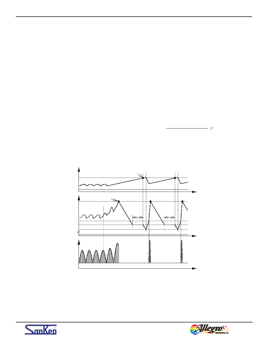
VCC Pin Overvoltage Protection. figure 33 shows the wave-
forms of the OVP function on the VCC pin. When the VCC pin
voltage with reference to the S/GND pin reaches and exceeds
VCC(OVP) = 31.5 V, OVP is activated and the device enters
intermittent oscillation mode operation. The startup circuit tries
to sustain VCC pin voltage at VCC(BIAS)1 = 11.0 V, but in the
meanwhile, the COMP pin voltage gradually increases and when
it reaches 2.0 V, it stops the startup circuit, and then VCC declines
further. When it reaches VCC(OFF) = 9.4 V, the startup sequence
begins again, and if the overvoltage condition still exists, the
same process described above is repeated and overall operation
enters the intermittent oscillation mode.
In addition, because VCC voltage is proportional to the output
voltage, it can be used to detect an output overvoltage event, such
as open load condition. In this situation, the detecting voltage is
expressed by the formula below:
=
VOUT(OVP)
31.5 (V)
VCC(normal operation)
VOUT(normal operation)
(4)
Figure 33. Waveforms when VCC pin OVP is being activated (LC551xD)
ID
S/GND
GND(ID)
2.0 V
VCOMP
OVP detected
VCC(OVP) = 31.5 V
VCC(ON) = 15.1 V
VCC(BIAS)1 = 11.0 V
VCC(OFF) = 9.4 V
VCC
Startup
circuit on
Startup
circuit on
VCOMP ≥ 2.0 V, startup circuit off
Time
相关PDF资料 |
PDF描述 |
|---|---|
| LC72137 | PLL FREQUENCY SYNTHESIZER, 40 MHz, PDIP22 |
| LC72137M | PLL FREQUENCY SYNTHESIZER, 40 MHz, PDSO20 |
| LC72137 | PLL FREQUENCY SYNTHESIZER, 40 MHz, PDIP22 |
| LC72137M | PLL FREQUENCY SYNTHESIZER, 40 MHz, PDSO20 |
| LC99403 | SPECIALTY ANALOG CIRCUIT, BGA180 |
相关代理商/技术参数 |
参数描述 |
|---|---|
| LC5523D | 制造商:Sanken Electric Co Ltd 功能描述:IC LED DRIVER ISO FLYBACK 8DIP |
| LC5523F | 制造商:Sanken Electric Co Ltd 功能描述:IC LED DVR ISO FLYBACK TO220-7 制造商:ALLEGRO 功能描述:LED Lighting Driver IC, Isolated 制造商:Allegro MicroSystems LLC 功能描述:LED Lighting Driver IC, Isolated |
| LC5525F | 制造商:Sanken Electric Co Ltd 功能描述:IC LED DVR ISO FLYBACK TO220-7 |
| LC552DIP | 制造商:未知厂家 制造商全称:未知厂家 功能描述:Analog IC |
| LC552SOIC | 制造商:未知厂家 制造商全称:未知厂家 功能描述:Analog IC |
发布紧急采购,3分钟左右您将得到回复。