- 您现在的位置:买卖IC网 > PDF目录79974 > LC72131K (SANYO SEMICONDUCTOR CO LTD) PLL FREQUENCY SYNTHESIZER, 40 MHz, PDIP22 PDF资料下载
参数资料
| 型号: | LC72131K |
| 厂商: | SANYO SEMICONDUCTOR CO LTD |
| 元件分类: | PLL合成/DDS/VCOs |
| 英文描述: | PLL FREQUENCY SYNTHESIZER, 40 MHz, PDIP22 |
| 封装: | 0.300 INCH, DIP-22 |
| 文件页数: | 7/22页 |
| 文件大小: | 200K |
| 代理商: | LC72131K |
LC72714W
No.6871-15/29
Structure of the Post-Correction Output Data <CCB Interface>
Post-error correction data can be output by using CCB address #FB. Although there are up to 288 bits of valid data that
can be output, it is possible to stop clock input (CL input) and set CE to the low level, and output the remaining data on
the next interrupt with no harmful effects whatsoever.
The maximum amount of data that can be output is 288 bits (36 bytes), and the contents of the status register (STAT)
and the block number register (BLNO) are added as the first two bytes.
The contents of the STAT and BLNO registers are output LSB first.
The post-correction data is output in order starting with the first bit in each single block of data.
The BIC code is not output.
The values of the output data are not guaranteed if multiple data read operations are performed for a single interrupt
signal (INT).
STAT (8 bits)
BLNO (8 bits)
Data section (176 bits) Post-error correction data
Layer 2 CRC (14 bits)
Parity (82 bits)
DO0 to DO7
DO8 to DO15
DO16 to DO191
DO192 to DO205
DO206 to DO287
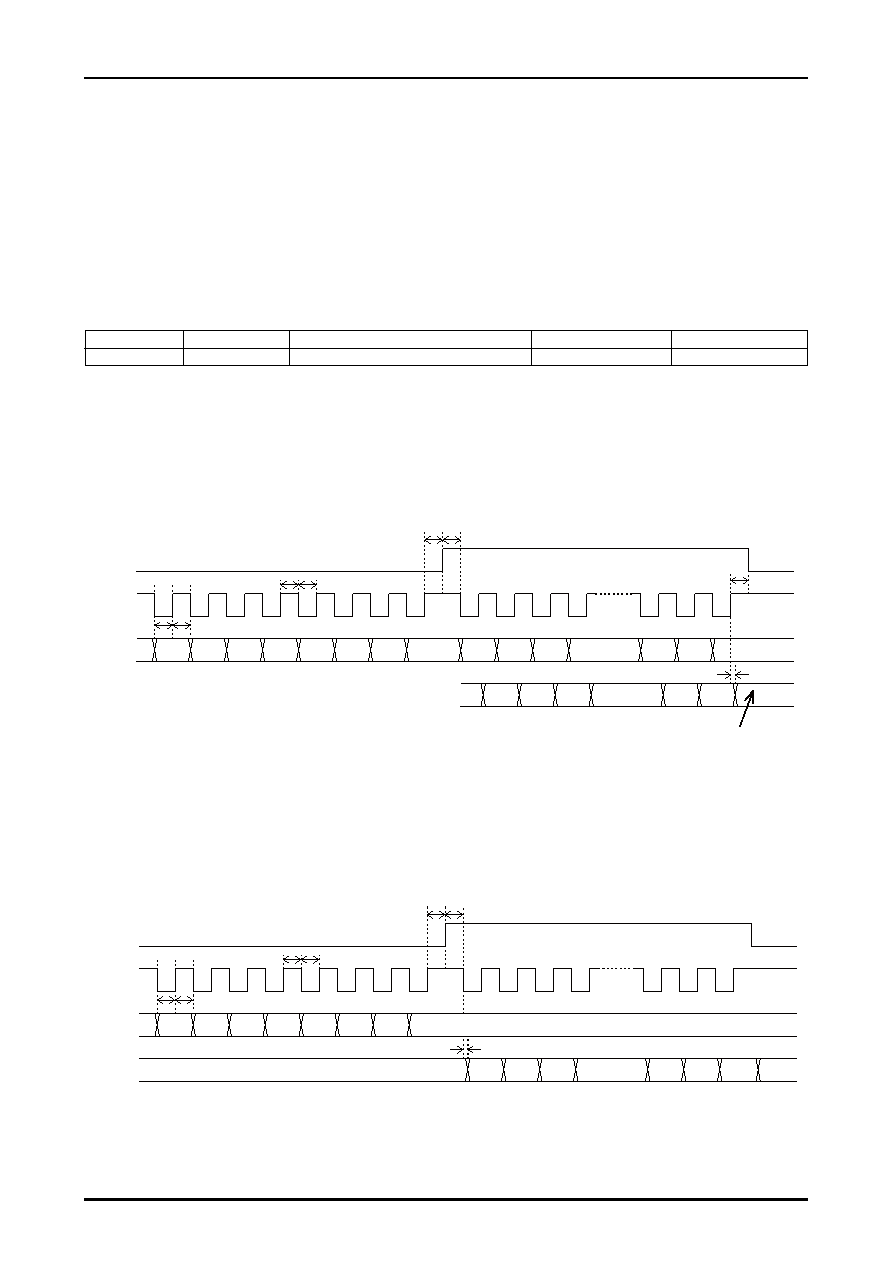
Layer 4 CRC Check Circuit <CCB Interface>
The basic outline of this operation is the same as that described in the Layer 4 CRC Detection Circuit <Parallel
Interface> section earlier in this document. The data group data used for this error detection operation is sent to the IC
using the CCB interface. The value #FC is used as the CCB address.
The data group data is transferred in 8-bit units. There is no upper limit on the amount of data that can be transferred
(the value N in the figure below), and the data transfer may be divided into multiple operations.
Register Output
The IC internal status and block number registers are special-purpose registers that can be read out by applications. (See
the discussion of the read register data update timing on page 11.)
The application inputs the CCB address #FD to DI. The status register data is output first followed by the block number
register data.
A3
N
N-1
N-2
CR2
CR1
CR0
A2
A1
A0
B3
B2
B1
B0
DI
CL
CE
CRC4 pin output
Note: The number of items, N, refers to
the number of 8-bit items.
CRC4 pin output after N items
have been transferred.
tCRC
tEH
tES
tEL
tCH
tCL
tHD
tSU
A3
BLN7
BLN6
BLN5
ST2
ST1
ST0
A2
A1
A0
B3
B2
B1
B0
DI
DO
CL
CE
tSU
tHD
tCH
tCL
tES
tEL
tDDO
相关PDF资料 |
PDF描述 |
|---|---|
| LPQ142-C | 4-OUTPUT 145 W AC-DC PWR FACTOR CORR MODULE |
| LH1001-2R-D1 | 1-OUTPUT AC-DC REG PWR SUPPLY MODULE |
| LH1783-2RD4 | 1-OUTPUT AC-DC REG PWR SUPPLY MODULE |
| LES020ZG-3N2V | 1-OUTPUT 15 W DC-DC REG PWR SUPPLY MODULE |
| LES020ZG-3N3N93V | 1-OUTPUT 15 W DC-DC REG PWR SUPPLY MODULE |
相关代理商/技术参数 |
参数描述 |
|---|---|
| LC72131K_12 | 制造商:SANYO 制造商全称:Sanyo Semicon Device 功能描述:PLL Frequency Synthesizer |
| LC72131KC-Z1 | 制造商:ON Semiconductor 功能描述:PLL FREQUENCY SYNTHESIZER - Bulk |
| LC72131KM | 制造商:SANYO 制造商全称:Sanyo Semicon Device 功能描述:PLL Frequency Synthesizer |
| LC72131KMA | 制造商:SANYO 制造商全称:Sanyo Semicon Device 功能描述:PLL Frequency Synthesizer |
| LC72131KMA-AE | 功能描述:时钟合成器/抖动清除器 RoHS:否 制造商:Skyworks Solutions, Inc. 输出端数量: 输出电平: 最大输出频率: 输入电平: 最大输入频率:6.1 GHz 电源电压-最大:3.3 V 电源电压-最小:2.7 V 封装 / 箱体:TSSOP-28 封装:Reel |
发布紧急采购,3分钟左右您将得到回复。