- 您现在的位置:买卖IC网 > PDF目录79974 > LC72131K (SANYO SEMICONDUCTOR CO LTD) PLL FREQUENCY SYNTHESIZER, 40 MHz, PDIP22 PDF资料下载
参数资料
| 型号: | LC72131K |
| 厂商: | SANYO SEMICONDUCTOR CO LTD |
| 元件分类: | PLL合成/DDS/VCOs |
| 英文描述: | PLL FREQUENCY SYNTHESIZER, 40 MHz, PDIP22 |
| 封装: | 0.300 INCH, DIP-22 |
| 文件页数: | 8/22页 |
| 文件大小: | 200K |
| 代理商: | LC72131K |
LC72714W
No.6871-16/29
Notes on Operation during Resets and in Standby Mode
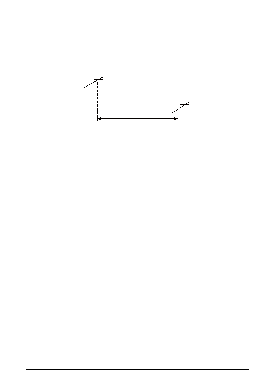
Reset Signal
The reset operation is executed when the supply voltage (VDD) rises above 2.5V (2.5V in the LC72710LW) and the
RST pin input level is held at or below VIL for 300ns or longer. (See the figure below.)
When power is first applied, or when power is removed and applied again, always apply a reset before using this IC.
Pin States during Reset
Low level:CLK16 (5), DATA (6), FLOCK (7), BLOCK (8), FCK (9), BCK (10)
High level: INT (33), RDY (16), CRC4 (11), DREQ (12)
Open: D0 (17) to D15 (32), DO (36)
Reset Operating Range
The states of the output pins as the result of a reset signal are stipulated in the "Pin States during Reset" item above.
The IC internal flip-flops are all reset. While the shift registers used for delay are also reset, the memory array is not
influenced by this operation. However, since memory is not refreshed, data cannot be retained. The crystal oscillator
circuit is not stopped.
Post-Reset Data Input
After a reset operation has completed, if at least one clock cycle (about 278ns when the IC's main clock is 3.6MHz)
elapses, the register write circuit will be functional. (That is, the IC can accept data.)
Notes on Standby Mode
The IC is set to standby mode by applying a high level to the STNBY pin. Since all IC operations are stopped in this
mode, the state is essentially equivalent to removing power from the IC. (Note that after clearing standby mode,
applications must wait the oscillator stabilization time before using the IC.)
The pin output states during standby mode are the same as those states during a reset as described above. The
internal VICS registers are cleared and the status flag values are not retained.
Output Conditions for Post-Error Correction Output (Default Mode)
(1) For each block (272 bits) of received data, the IC applies (272, 190) code error correction and a layer 2 CRC
error check. After the error correction has completed, the IC prepares to transfer the data to the CPU and
outputs an interrupt signal from the INT pin. This is referred to as horizontal correction output.
(2) Note that under the default operating conditions, this interrupt signal is not output unless the corresponding
output data meets the following three conditions.
Error correction completed correctly and no errors were discovered in the layer 2 CRC check.
The data was received in both block and frame synchronization.
The data is packet data.
(3) If the data could not be corrected in horizontal correction, product code correction is performed in frame units
and a second horizontal correction operation is performed for this data that could not be corrected by the first
horizontal correction. This sequence of operations is called vertical correction.
The output conditions for data that can be acquired after vertical correction are as follows.
The data that could not be corrected by horizontal correction only, but that was corrected by vertical
correction.
The data is packet data.
Continued on next page.
RST
2.5V
VIL(0.3VDD)
VIH
300ns(min)
VDD voltage
相关PDF资料 |
PDF描述 |
|---|---|
| LPQ142-C | 4-OUTPUT 145 W AC-DC PWR FACTOR CORR MODULE |
| LH1001-2R-D1 | 1-OUTPUT AC-DC REG PWR SUPPLY MODULE |
| LH1783-2RD4 | 1-OUTPUT AC-DC REG PWR SUPPLY MODULE |
| LES020ZG-3N2V | 1-OUTPUT 15 W DC-DC REG PWR SUPPLY MODULE |
| LES020ZG-3N3N93V | 1-OUTPUT 15 W DC-DC REG PWR SUPPLY MODULE |
相关代理商/技术参数 |
参数描述 |
|---|---|
| LC72131K_12 | 制造商:SANYO 制造商全称:Sanyo Semicon Device 功能描述:PLL Frequency Synthesizer |
| LC72131KC-Z1 | 制造商:ON Semiconductor 功能描述:PLL FREQUENCY SYNTHESIZER - Bulk |
| LC72131KM | 制造商:SANYO 制造商全称:Sanyo Semicon Device 功能描述:PLL Frequency Synthesizer |
| LC72131KMA | 制造商:SANYO 制造商全称:Sanyo Semicon Device 功能描述:PLL Frequency Synthesizer |
| LC72131KMA-AE | 功能描述:时钟合成器/抖动清除器 RoHS:否 制造商:Skyworks Solutions, Inc. 输出端数量: 输出电平: 最大输出频率: 输入电平: 最大输入频率:6.1 GHz 电源电压-最大:3.3 V 电源电压-最小:2.7 V 封装 / 箱体:TSSOP-28 封装:Reel |
发布紧急采购,3分钟左右您将得到回复。