- 您现在的位置:买卖IC网 > PDF目录30730 > LC72131KM (SANYO SEMICONDUCTOR CO LTD) PLL FREQUENCY SYNTHESIZER, 40 MHz, PDSO20 PDF资料下载
参数资料
| 型号: | LC72131KM |
| 厂商: | SANYO SEMICONDUCTOR CO LTD |
| 元件分类: | PLL合成/DDS/VCOs |
| 英文描述: | PLL FREQUENCY SYNTHESIZER, 40 MHz, PDSO20 |
| 封装: | 0.300 INCH, MFP-20 |
| 文件页数: | 20/22页 |
| 文件大小: | 200K |
| 代理商: | LC72131KM |
LC72131K, 72131KM
No.A0788-7/22
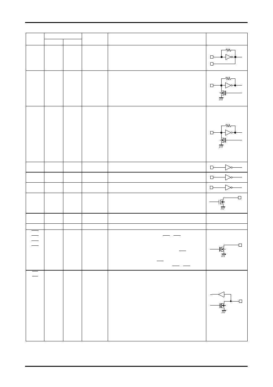
Pin Functions
Pin No.
Symbol
LC72131K
LC72131KM
Type
Functions
Circuit configuration
XIN
XOUT
1
22
1
20
X'tal OSC
Crystal resonator connection
(4.5MHz/7.2MHz)
FMIN
16
14
Local
oscillator
signal input
FMIN is selected when the serial data input DVS bit is set to 1.
The input frequency range is from 10 to 160MHz.
The input signal passes through the internal divide-by-two
prescaler and is input to the swallow counter.
The divisor can be in the range 272 to 65535. However,
since the signal has passed through the divide-by-two
prescaler, the actual divisor is twice the set value.
AMIN
15
13
Local
oscillator
signal input
AMIN is selected when the serial data input DVS bit is set to 0.
When the serial data input SNS bit is set to 1:
The input frequency range is 2 to 40MHz.
The signal is directly input to the swallow counter.
The divisor can be in the range 272 to 65535, and the divisor
used will be the value set.
When the serial data input SNS bit is set to 0:
The input frequency range is 0.5 to 10MHz.
The signal is directly input to a 12-bit programmable divider.
The divisor can be in the range 4 to 4095, and the divisor
used will be the value set.
CE
3
2
Chip enable
Set this pin high when inputting (DI) or outputting (DO) serial
data.
DI
4
3
Input data
Inputs serial data transferred from the controller to the LC72131.
CL
5
4
Clock
Used as the synchronization clock when inputting (DI) or
outputting (DO) serial data.
DO
6
5
Output data
Outputs serial data transferred from the LC72131 to the
controller.
The content of the output data is determined by the serial data
DOC0 to DOC2.
VDD
17
15
Power supply
The LC72131 power supply pin (VDD=4.5 to 5.5V)
The power on reset circuit operates when power is first applied.
-
VSS
21
19
Ground
The LC72131 ground
-
BO1
BO2
BO3
BO4
7
8
9
10
6
7
8
9
Output port
Dedicated output pins
The output states are determined by BO1 to BO4 bits in
the serial data.
Data: 0=open, 1=low
A time base signal (8Hz) can be output from the BO1 pin.
(When the serial data TBC bit is set to 1.)
Care is required when using the BO1 pin, since it has a higher on
impedance that the other output ports (pins BO2 to BO4).
IO1
IO2
11
13
10
12
I/O port
I/O dual-use pins
The direction (input or output) is determined by bits IOC1 and
IOC2 in the serial data.
Data: 0=input port, 1=output port
When specified for use as input ports:
The state of the input pin is transmitted to the controller over
the DO pin.
Input state: low=0 data value
high=1 data value
When specified for use as output ports:
The output states are determined by the IO1 and IO2 bits in
the serial data.
Data: 0=open, 1=low
These pins function as input pins following a power on reset.
Continued on next page.
S
相关PDF资料 |
PDF描述 |
|---|---|
| LC72133V | PLL FREQUENCY SYNTHESIZER, 40 MHz, PDSO20 |
| LC72133M | PLL FREQUENCY SYNTHESIZER, 40 MHz, PDSO20 |
| LC7219M | PLL FREQUENCY SYNTHESIZER, 160 MHz, PDSO24 |
| LC7230-8221 | SPECIALTY CONSUMER CIRCUIT, PQFP80 |
| LC7230-8272 | SPECIALTY CONSUMER CIRCUIT, PQFP80 |
相关代理商/技术参数 |
参数描述 |
|---|---|
| LC72131KMA | 制造商:SANYO 制造商全称:Sanyo Semicon Device 功能描述:PLL Frequency Synthesizer |
| LC72131KMA-AE | 功能描述:时钟合成器/抖动清除器 RoHS:否 制造商:Skyworks Solutions, Inc. 输出端数量: 输出电平: 最大输出频率: 输入电平: 最大输入频率:6.1 GHz 电源电压-最大:3.3 V 电源电压-最小:2.7 V 封装 / 箱体:TSSOP-28 封装:Reel |
| LC72131M | 制造商:SANYO 制造商全称:Sanyo Semicon Device 功能描述:AM/FM PLL Frequency Synthesizer |
| LC72131MDTRM | 制造商:Panasonic Industrial Company 功能描述:IC |
| LC72132 | 制造商:SANYO 制造商全称:Sanyo Semicon Device 功能描述:AM/FM PLL Frequency Synthesizer |
发布紧急采购,3分钟左右您将得到回复。