- 您现在的位置:买卖IC网 > PDF目录30730 > LC72131KM (SANYO SEMICONDUCTOR CO LTD) PLL FREQUENCY SYNTHESIZER, 40 MHz, PDSO20 PDF资料下载
参数资料
| 型号: | LC72131KM |
| 厂商: | SANYO SEMICONDUCTOR CO LTD |
| 元件分类: | PLL合成/DDS/VCOs |
| 英文描述: | PLL FREQUENCY SYNTHESIZER, 40 MHz, PDSO20 |
| 封装: | 0.300 INCH, MFP-20 |
| 文件页数: | 6/22页 |
| 文件大小: | 200K |
| 代理商: | LC72131KM |
LC72714W
No.6871-14/29
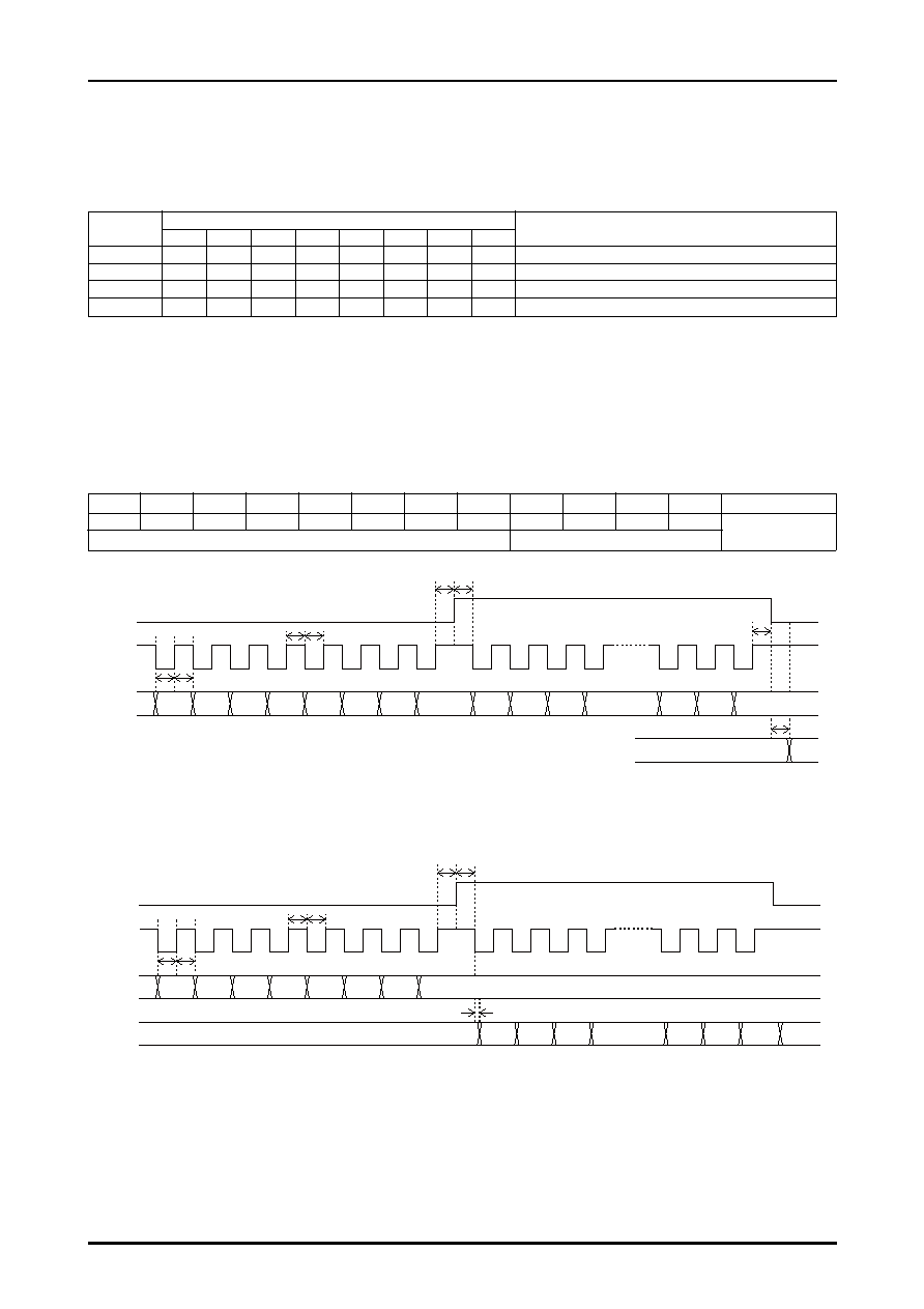
CPU Interface <CCB Mode>
CCB Format
Data is input and output using the CCB (Computer Control Bus) format, which is Sanyo’s audio IC serial bus format.
This IC uses an 8-bit address CCB with the address shown below. The CCB address is sent while CE is low, and the
CCB I/O mode is determined when CE is set high.
I/O mode
CCB address
Item
B0
B1
B2
B3
A0
A1
A2
A3
Input
0
1
0
1
16-bit control data input
Output
1
0
1
Data corresponding to the number of clock (CL) cycles is output
Input
0
1
Data input mode for the layer 4 CRC detection circuit (8-bit units)
Output
1
0
1
Register output only
Data input (Register write)
Data is stored in an IC internal register. The CCB address #FA and 16 bits of data (DI0 to DI15) are input to the DI pin.
The bits are assigned as follows. Although DI12 to DI15 are unused data, arbitrary values must be provided to complete
a full 16 bits of data.
See the “Control Register” section earlier in this document for details on the register contents and addresses.
Details on writing to the layer 4 CRC check register are described later in this document. (The CCB address #FC is used
for this function.)
DI0
DI1
DI2
DI3
DI4
DI5
DI6
DI7
DI8
DI9
DI10
DI11
DI12 to DI15
BIT0
BIT1
BIT2
BIT3
BIT4
BIT5
BIT6
BIT7
BIT0
BIT1
BIT2
BIT3
Unused data
(LSB)
Input data (8 bits)
(MSB)
Register address
Data Output (Post-correction data output)
The IC outputs packet data to which error correction processing has be applied. The application inputs the CCB address
#FB to DI.
*: The DO pin is normally left open.
Since the DO pin is an n-channel open-drain output, the data change time from a low-level output to a high-level
output differs due to the pull-up resistor.
Internal data latch operation
A3
DI15
DI14
DI13
DI2
DI1
DI0
A2
A1
A0
B3
B2
B1
B0
DI
CL
CE
tHD
tSU
tCH
tCL
tEL
tES
tLC
tEH
A3
DO287
DO286
DO285
DO2
DO1
DO0
A2
A1
A0
B3
B2
B1
B0
DI
DO
CL
CE
tEL
tES
tCH
tCL
tSU
tHD
tDDO
相关PDF资料 |
PDF描述 |
|---|---|
| LC72133V | PLL FREQUENCY SYNTHESIZER, 40 MHz, PDSO20 |
| LC72133M | PLL FREQUENCY SYNTHESIZER, 40 MHz, PDSO20 |
| LC7219M | PLL FREQUENCY SYNTHESIZER, 160 MHz, PDSO24 |
| LC7230-8221 | SPECIALTY CONSUMER CIRCUIT, PQFP80 |
| LC7230-8272 | SPECIALTY CONSUMER CIRCUIT, PQFP80 |
相关代理商/技术参数 |
参数描述 |
|---|---|
| LC72131KMA | 制造商:SANYO 制造商全称:Sanyo Semicon Device 功能描述:PLL Frequency Synthesizer |
| LC72131KMA-AE | 功能描述:时钟合成器/抖动清除器 RoHS:否 制造商:Skyworks Solutions, Inc. 输出端数量: 输出电平: 最大输出频率: 输入电平: 最大输入频率:6.1 GHz 电源电压-最大:3.3 V 电源电压-最小:2.7 V 封装 / 箱体:TSSOP-28 封装:Reel |
| LC72131M | 制造商:SANYO 制造商全称:Sanyo Semicon Device 功能描述:AM/FM PLL Frequency Synthesizer |
| LC72131MDTRM | 制造商:Panasonic Industrial Company 功能描述:IC |
| LC72132 | 制造商:SANYO 制造商全称:Sanyo Semicon Device 功能描述:AM/FM PLL Frequency Synthesizer |
发布紧急采购,3分钟左右您将得到回复。