- 您现在的位置:买卖IC网 > PDF目录30730 > LC7219M PLL FREQUENCY SYNTHESIZER, 160 MHz, PDSO24 PDF资料下载
参数资料
| 型号: | LC7219M |
| 元件分类: | PLL合成/DDS/VCOs |
| 英文描述: | PLL FREQUENCY SYNTHESIZER, 160 MHz, PDSO24 |
| 封装: | MFP-24 |
| 文件页数: | 8/12页 |
| 文件大小: | 212K |
| 代理商: | LC7219M |
LC7219, 7219M
No.3661–5/12
Table 1. Input data bits
Table 2. Reference frequency selection
s
t
i
Be
m
a
Nn
o
i
t
p
i
r
c
s
e
Ds
t
i
b
d
e
t
a
l
e
R
6
1
o
t
1D0
D
o
t
5
1
o
i
t
a
r
e
d
i
v
i
d
e
l
b
a
m
a
r
g
o
r
P
D 5
1
.
6
e
l
b
a
t
n
i
n
w
o
h
s
a
s
g
a
l
f
P
S
d
n
a
V
D
e
h
t
f
o
g
n
i
t
e
s
e
h
t
y
b
d
e
n
i
m
r
e
t
e
d
s
i
b
s
l
e
h
T
.
b
s
m
e
h
t
s
i
D0
D
o
t
3
D
f
i
d
e
r
o
n
g
i
e
r
a
4
.
b
s
l
e
h
t
s
i
P
S
,
V
D
3
2
o
t
7
1O0
O
o
t
6
a
t
a
d
t
r
o
p
t
u
p
t
u
O
s
t
i
b
a
t
a
D
0
O
o
t
6
,
1
s
i
t
i
b
a
t
a
d
a
n
e
h
W
.
y
l
e
v
i
t
c
e
p
s
e
r
,
s
t
r
o
p
6
T
U
O
o
t
0
T
U
O
e
h
t
o
t
n
i
d
e
h
c
t
a
l
e
r
a
r
o
f
d
e
s
u
e
b
n
a
c
s
t
u
p
t
u
o
e
s
e
h
T
.
H
G
I
H
,
0
n
e
h
w
d
n
a
,
W
O
L
s
i
n
i
p
t
u
p
t
u
o
g
n
i
d
n
o
p
s
e
r
o
c
e
h
t
.
n
o
i
t
c
e
l
e
s
d
n
a
b
y
c
n
e
u
q
e
r
f
O
e
h
t
,
1
s
i
B
T
f
I
0
.
0
T
U
O
n
o
t
u
p
t
u
o
s
i
l
a
n
g
i
s
e
s
a
b
e
m
i
t
z
H
8
e
h
t
d
n
a
d
e
r
o
n
g
i
s
i
t
i
b
B
T
4
2N
E
T
C
e
l
b
a
n
e
r
e
t
n
u
o
c
e
s
o
p
r
u
p
-
l
a
r
e
n
e
G
e
r
a
s
t
u
n
i
R
T
C
L
d
n
a
R
T
C
H
e
h
t
d
n
a
t
e
s
e
r
s
i
r
e
t
n
u
o
c
e
s
o
p
r
u
p
-
l
a
r
e
n
e
g
t
i
b
-
0
2
e
h
t
,
0
s
i
N
E
T
C
n
e
h
W
r
o
R
T
C
H
n
o
l
a
n
g
i
s
e
h
t
d
n
a
d
e
l
b
a
n
e
s
i
r
e
t
n
u
o
c
e
h
t
,
1
s
i
g
a
l
f
N
E
T
C
e
h
t
n
e
h
W
.
d
n
u
o
r
g
o
t
d
e
ll
u
p
e
b
d
l
u
o
h
s
t
u
p
t
u
o
r
e
t
n
u
o
c
e
s
o
p
r
u
p
-
l
a
r
e
n
e
g
e
h
t
a
h
t
e
t
o
N
.
d
e
r
u
s
a
e
m
s
i
,
C
S
y
b
d
e
t
c
e
l
e
s
,
R
T
C
L
.
0
o
t
e
s
i
N
E
T
C
e
r
o
f
e
b
r
e
ll
o
r
t
n
o
c
l
a
n
r
e
t
x
e
h
t
o
t
d
e
r
e
f
s
n
a
r
t
T
G
,
F
S
,
C
S
8
2
o
t
5
2R0
R
o
t
3
t
c
e
l
e
s
y
c
n
e
u
q
e
r
f
e
c
n
e
r
e
f
e
R
s
t
i
B
0
R
o
t
3
e
h
t
n
e
h
W
.
2
e
l
b
a
t
n
i
n
w
o
h
s
a
y
c
n
e
u
q
e
r
f
e
c
n
e
r
e
f
e
r
e
h
t
c
e
l
e
s
r
o
L
P
e
h
t
e
l
b
a
s
i
d
n
a
,
d
n
u
o
r
g
o
t
d
e
ll
u
p
e
r
a
N
I
M
F
d
n
a
N
I
M
A
,
d
e
p
o
t
s
i
r
e
d
i
v
i
d
e
l
b
a
m
a
r
g
o
r
p
e
h
t
,
d
e
l
b
a
s
i
d
s
i
L
P
.
e
c
n
a
d
e
p
m
i
h
g
i
h
e
m
o
c
e
b
s
t
u
p
t
u
o
p
m
u
p
-
e
g
r
a
h
c
e
h
t
0
3
,
9
2P
S
,
V
D
t
c
e
l
e
s
y
t
i
v
i
t
i
s
n
e
s
d
n
a
t
c
e
l
e
s
r
e
d
i
v
i
D
n
e
h
w
e
g
n
a
r
y
c
n
e
u
q
e
r
f
t
u
p
n
i
e
h
t
s
t
c
e
l
e
s
P
S
.
N
I
M
A
r
o
N
I
M
F
t
u
p
n
i
r
o
t
a
ll
i
c
s
o
-
l
a
c
o
l
e
h
t
c
e
l
e
s
V
D
.
6
e
l
b
a
t
n
i
n
w
o
h
s
a
d
e
t
c
e
l
e
s
i
N
I
M
A
2
3
,
1
3F
S
,
C
S
t
c
e
l
e
s
t
n
e
m
e
r
u
s
a
e
m
d
o
i
r
e
p
/
y
c
n
e
u
q
e
r
f
d
n
a
t
c
e
l
e
s
t
u
p
n
i
r
e
t
n
u
o
c
e
s
o
p
r
u
p
-
l
a
r
e
n
e
G
n
e
h
w
t
n
e
m
e
r
u
s
a
e
m
d
o
i
r
e
p
r
o
y
c
n
e
u
q
e
r
f
s
t
c
e
l
e
s
F
S
.
t
u
p
n
i
r
e
t
n
u
o
c
e
s
o
p
r
u
p
-
l
a
r
e
n
e
g
e
h
t
s
t
c
e
l
e
s
C
S
y
c
n
e
u
q
e
r
f
n
i
s
i
r
e
t
n
u
o
c
e
h
t
,
d
e
t
c
e
l
e
s
i
R
T
C
H
n
e
h
W
.
7
e
l
b
a
t
n
i
n
w
o
h
s
a
d
e
t
c
e
l
e
s
i
R
T
C
L
.
e
d
o
m
t
n
e
m
e
r
u
s
a
e
m
T
G
,
N
E
T
C
3
3T
G
t
c
e
l
e
s
l
a
v
r
e
t
n
i
e
m
i
t
r
e
t
n
u
o
c
e
s
o
p
r
u
p
-
l
a
r
e
n
e
G
n
e
h
W
.
d
e
r
u
s
a
e
m
e
b
o
t
s
d
o
i
r
e
p
f
o
r
e
b
m
u
n
e
h
t
r
o
l
a
v
r
e
t
n
i
e
m
i
t
n
e
m
e
r
u
s
a
e
m
e
h
t
s
t
c
e
l
e
s
T
G
t
i
B
.
d
e
t
c
e
l
e
s
i
d
o
i
r
e
p
1
r
o
s
m
0
6
,
0
=
T
G
n
e
h
w
d
n
a
,
d
e
t
c
e
l
e
s
e
r
a
s
d
o
i
r
e
p
2
r
o
s
m
0
3
n
e
h
t
,
1
=
T
G
F
S
,
C
S
,
N
E
T
C
4
3B
T
e
l
b
a
n
e
t
u
p
t
u
o
e
s
a
b
e
m
i
T
O
e
h
T
.
0
T
U
O
n
o
t
u
p
t
u
o
s
i
l
a
n
g
i
s
e
s
a
b
e
m
i
t
e
l
c
y
c
y
t
u
d
%
0
4
,
z
H
8
e
h
t
,
1
s
i
B
T
n
e
h
W
0
s
i
s
t
i
b
.
d
e
r
o
n
g
i
O0
6
3
,
5
3T0 T
, 1
s
t
i
b
l
o
r
t
n
o
c
t
s
e
T
s
t
i
BT0
T
o
t
1
.
n
o
i
t
a
r
e
p
o
l
a
m
r
o
n
r
o
f
0
o
t
e
s
e
r
a
d
n
a
g
n
i
t
s
e
t
e
c
i
v
e
d
r
o
f
d
e
s
u
e
r
a
Table 2. Reference frequency selection–continued
R0
R1
R2
R3
)
z
H
k
(
y
c
n
e
u
q
e
r
f
e
c
n
e
r
e
f
e
R
0000
0
1
0001
0
5
0010
5
2
0011
5
2
0100
5
.
2
1
0101
5
2
.
6
0110
5
2
1
.
3
0111
5
2
1
.
3
R0
R1
R2
R3
)
z
H
k
(
y
c
n
e
u
q
e
r
f
e
c
n
e
r
e
f
e
R
1000
0
1
1001
9
1010
5
1011
1
1100
t
i
b
i
h
n
i
L
P
1101
1110
1111
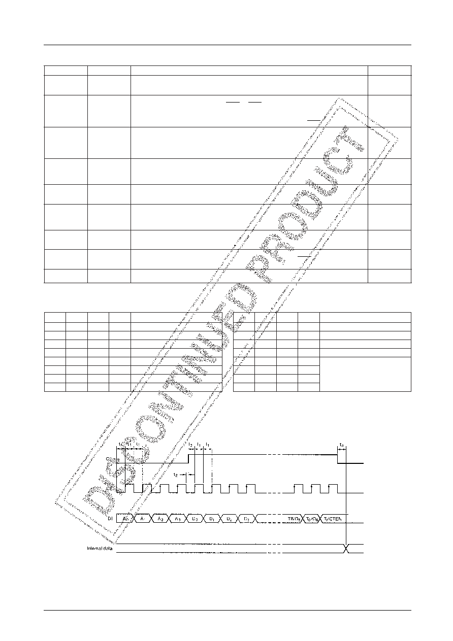
Serial Data Input Timing
The timing for the serial data input is shown in figure 2. The first four bits, A0 to A3, are the mode select bits.
In 36-bit transfer mode, the final data bits are T0 and T1, and in 24-bit transfer mode, O6 and CTEN.
Note
t1≥1.5s, t2≥0s, t3≥1.5s, t4<1.5s
Figure 2. Input timing
The reference frequency is selected by bits R0 to R3 as shown in table 2.
相关PDF资料 |
PDF描述 |
|---|---|
| LC7230-8221 | SPECIALTY CONSUMER CIRCUIT, PQFP80 |
| LC7230-8272 | SPECIALTY CONSUMER CIRCUIT, PQFP80 |
| LC72323-XXXX | SPECIALTY CONSUMER CIRCUIT, PQFP80 |
| LC723341E | SPECIALTY CONSUMER CIRCUIT, PQFP64 |
| LC723341E | SPECIALTY CONSUMER CIRCUIT, PQFP64 |
相关代理商/技术参数 |
参数描述 |
|---|---|
| LC7220 | 制造商:未知厂家 制造商全称:未知厂家 功能描述: |
| LC7221 | 制造商:未知厂家 制造商全称:未知厂家 功能描述: |
| LC7222 | 制造商:未知厂家 制造商全称:未知厂家 功能描述: |
| LC7223 | 制造商:未知厂家 制造商全称:未知厂家 功能描述: |
| LC7225 | 制造商:未知厂家 制造商全称:未知厂家 功能描述: |
发布紧急采购,3分钟左右您将得到回复。