- 您现在的位置:买卖IC网 > PDF目录30731 > LC72706E SPECIALTY CONSUMER CIRCUIT, PQFP44 PDF资料下载
参数资料
| 型号: | LC72706E |
| 元件分类: | 消费家电 |
| 英文描述: | SPECIALTY CONSUMER CIRCUIT, PQFP44 |
| 封装: | QFP-44 |
| 文件页数: | 3/15页 |
| 文件大小: | 164K |
| 代理商: | LC72706E |
To prevent unnecessary error correction, the vertical correction is not applied to packets that were fully corrected by
horizontal correction or to packets that had no errors.
Vertical correction is executed when all packet data in the object data was received while frame synchronization was
established and not all of the packet (block) data was corrected by horizontal correction. Vertical correction is not
performed if a whole frame of data with no errors is received, or if the frame was not synchronized. Also, the
corresponding post-vertical correction output data is not output.
All data can be output, regardless of the correction complete/incomplete, synchronized/unsynchronized reception,
data/packet status or other conditions by setting bit 5 (INT) in the control register to 1.
CPU Interface Basic Restrictions
To save internal memory, this IC uses the smallest possible output buffer. Since the data that the IC receives is written to
memory without any breaks, if data readout is delayed post-correction data that should be read out will be overwritten by
the next data to be output. The output timings in this IC for post-correction (horizontal and vertical) data are stipulated as
follows.
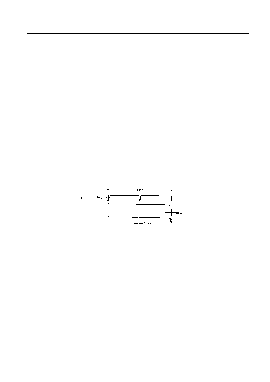
When preparation of the output data has completed, the IC issues a transfer request by setting the INT pin low.
For data output, there are periods in which only horizontal data can be output and periods in which both horizontal data
and vertical data can be output.
Data transfers must be completed within about 9 ms after the INT pin goes low. For periods in which only post-
horizontal correction data can be output, data can be transferred over a period of about 18 ms. Even if the CPU is in the
midst of a read operation, the next output data will be written to the output buffer after the specified period elapses.
Only one block of data can be read for a single transfer request (INT) for both vertical and horizontal correction. After
vertical correction processing completes, the post-vertical correction data is output in order starting with block number
1, and the parity block data is not output.
Figure 2 Basic Interface Timing
Notes on Data Output Timing (The relationship with the received data)
Figure 3 shows the timing relationship between the received data and the interrupt control signal INT. However, the
delay component relative to the actually received signal due to the demodulation operations in the MSK demodulation
block is ignored. Block synchronization is established by recognizing the BIC code. As shown in figure 3, the data for the
nth packet can be output during the reception of the next packet, packet number n + 1.
Figure 4 shows the output timing for vertical correction data. Vertical correction is used when the data for a whole frame
is stored in memory, frame synchronization is established, and furthermore horizontal correction was not able to correct
all the packet data. The timing for the start of vertical correction execution is the head of the frame. During reception of
packets 1 to 28 in the nth frame, horizontal correction is performed on each packet, data is passed to the CPU, and the
remaining unused processing time during that interval is used to apply vertical correction to the data from the previous
frame (frame n – 1). The post-vertical correction data (190 blocks of data) is output in order starting when the 29th packet
(block) is received at the rate of one block of output data for every block received. Of the data in the FM multiplex
broadcast frame structure, only the data in the data blocks is output, and the 190th block (the last data block) is output
while the 218th block is being received. As discussed previously (page 10), of the post-vertical correction output data, the
packet data for which horizontal correction completed fully is not output (the INT signal is not issued). However, it is not
the case that the vertical output is speeded up by the amount of the packet data that is not output. For example, if data
packets 1 to 100 were fully corrected in horizontal correction, the point that the 101st post-vertical correction packet data
is output will not be the reception position block number 29 in figure 4, but the reception position of packet data number
129.
No. 5745-11/15
LC72706E
Only horizontal
data output
Horizontal data
output period
Period when
data cannot be
guaranteed
Horizontal data
output period
Vertical data output period
Horizontal and
vertical data output
相关PDF资料 |
PDF描述 |
|---|---|
| LC72707E | SPECIALTY CONSUMER CIRCUIT, PQFP44 |
| LC72708E | SPECIALTY CONSUMER CIRCUIT, PQFP44 |
| LC72708E | SPECIALTY CONSUMER CIRCUIT, PQFP44 |
| LC72709E | SPECIALTY CONSUMER CIRCUIT, PQFP44 |
| LC72709W | SPECIALTY CONSUMER CIRCUIT, PQFP64 |
相关代理商/技术参数 |
参数描述 |
|---|---|
| LC72707 | 制造商:SANYO 制造商全称:Sanyo Semicon Device 功能描述:FM Multiplex Receiver IC Supporting All Worldwide Standards |
| LC72707E | 制造商:SANYO 制造商全称:Sanyo Semicon Device 功能描述:FM Multiplex Receiver IC Supporting All Worldwide Standards |
| LC72708 | 制造商:SANYO 制造商全称:Sanyo Semicon Device 功能描述:FM Multiplex Broadcast Reception IC for Mobile VICS Systems |
| LC72708E | 制造商:SANYO 制造商全称:Sanyo Semicon Device 功能描述:FM Multiplex Broadcast Reception IC for Mobile VICS Systems |
| LC72709 | 制造商:SANYO 制造商全称:Sanyo Semicon Device 功能描述:FM Multiplex Reception IC for Mobile Systems |
发布紧急采购,3分钟左右您将得到回复。