- 您现在的位置:买卖IC网 > PDF目录30731 > LC72706E SPECIALTY CONSUMER CIRCUIT, PQFP44 PDF资料下载
参数资料
| 型号: | LC72706E |
| 元件分类: | 消费家电 |
| 英文描述: | SPECIALTY CONSUMER CIRCUIT, PQFP44 |
| 封装: | QFP-44 |
| 文件页数: | 8/15页 |
| 文件大小: | 164K |
| 代理商: | LC72706E |
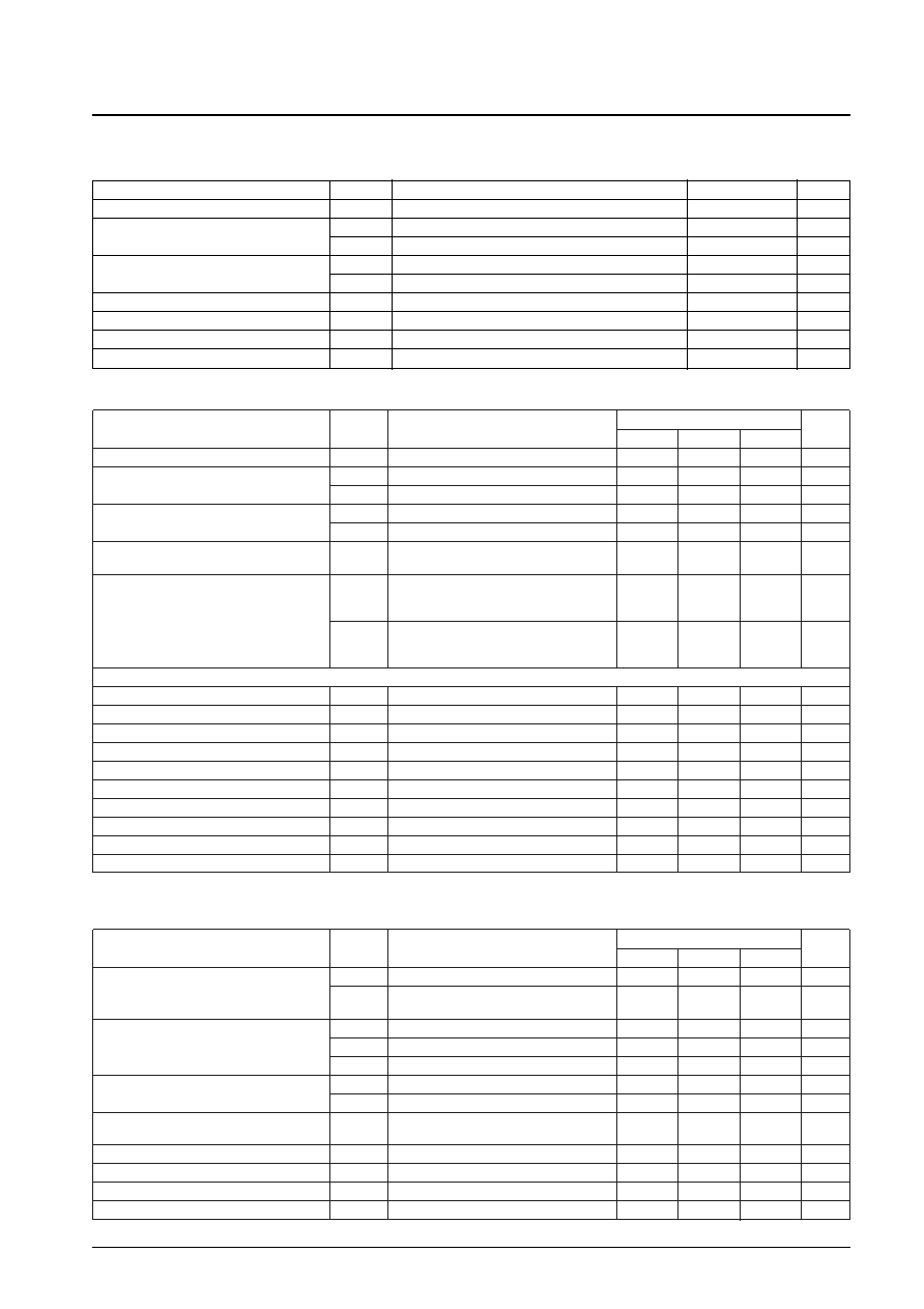
No. 5745-2/15
LC72706E
Parameter
Symbol
Conditions
Ratings
Unit
Maximum supply voltage
VDD max
–0.3 to +7.0
V
Input voltage
VIN1
CE, CL, DI, RST, STNBY
–0.3 to +7.0
V
VIN2
Pins other than VIN1
–0.3 to VDD +0.3
V
Output voltage
VOUT1
DO
–0.3 to +7.0
V
VOUT2
Pins other than VOUT1
–0.3 to VDD +0.3
V
Output current
IOUT
BLOCK, FLOCK, DO
0 to 4.0
mA
Allowable power dissipation
Pd max
Ta
≤ 85°C
400
mW
Operating temperature
Topr
–40 to +85
°C
Storage temperature
Tstg
–55 to +125
°C
Specifications
Absolute Maximum Ratings at Ta = 25°C, VSS = 0 V
Parameter
Symbol
Conditions
Ratings
Unit
min
typ
max
Supply voltage
VDD
2.7
5.5
V
Input high-level voltage
VIH1
CL, CE, DI, RST, STNBY
0.7 VDD
5.5
V
VIH2
MSK
0.7 VDD
VDD
V
Input low-level voltage
VIL1
Applies to the same pins as VIH1
VSS
0.3 VDD
V
VIL2
Applies to the same pins as VIH2
VSS
0.3 VDD
V
Oscillator frequency
FOSC
This IC operates at frequencies within a
7.2
MHz
±250 ppm precision.
With a capacitance-coupled sine wave input
VXI
to XIN
400
1500
mVrms
Input sensitivity
VDD = +4.5 V to 5.5 V
With a capacitance-coupled sine wave input
VXI
to XIN
400
900
mVrms
VDD = +2.7 V to 3.6 V
[Serial I/O*]
Clock low-level time
tCL
CL
0.7
s
Clock high-level time
tCH
CL
0.7
s
Data setup time
tSU
CL, DI
0.7
s
Data hold time
tHD
CL, DI
0.7
s
CE wait time
tEL
CL, CE
0.7
s
CE setup time
tES
CL, CE
0.7
s
CE hold time
tEH
CL, CE
0.7
s
Data latch change time
tLC
CE
0.7
s
Data output time
tDD0
DO, CL
277
555
ns
Layer 4 CRC change time
tCRC
CRC4, CL
0.7
s
Allowable Operating Ranges at Ta = –40 to 85°C, VSS = 0 V
Note *: See the serial data timing chart.
Parameter
Symbol
Conditions
Ratings
Unit
min
typ
max
VOH1
IO = 1 mA, FLICK
VDD – 1.0
V
Output high-level voltage
VOH2
IO = 2 mA, BLOCK, FLOCK, INT, CLK16,
VDD – 0.4
V
DATA
VOL1
IO = 1 mA, applies to the same pins as VOH1
1.0
V
Output low-level voltage
VOL2
IO = 2 mA, applies to the same pins as VOH2
0.4
V
VOL3
IO = 2 mA, DO
0.4
V
Input high-level current
IIH1
VIN = 5.5 V, CE, CL, DI, RST, STNBY
1.0
A
IIH2
VIN = VDD, input pins other than IIH1
1.0
A
Input low-level current
IIL
VIN = VSS, MSK, CL, CE, DI, RST, STNBY,
–1
A
TP0 to TP8, TPC1 to 2, TOSEL1 to 2, TEST
Output off leakage current
IOFF
VO = VDD, DO
5
A
Hysteresis voltage
VHIS
MSK, CL, CE, DI, RST, STNBY
0.1 VDD
V
Internal feedback resistor
Rf
XIN, XOUT
1.0
M
Current drain
IDD
16
25
mA
Electrical Characteristics (1) at VDD = +4.5 to +5.5 V, in the allowable operating ranges
相关PDF资料 |
PDF描述 |
|---|---|
| LC72707E | SPECIALTY CONSUMER CIRCUIT, PQFP44 |
| LC72708E | SPECIALTY CONSUMER CIRCUIT, PQFP44 |
| LC72708E | SPECIALTY CONSUMER CIRCUIT, PQFP44 |
| LC72709E | SPECIALTY CONSUMER CIRCUIT, PQFP44 |
| LC72709W | SPECIALTY CONSUMER CIRCUIT, PQFP64 |
相关代理商/技术参数 |
参数描述 |
|---|---|
| LC72707 | 制造商:SANYO 制造商全称:Sanyo Semicon Device 功能描述:FM Multiplex Receiver IC Supporting All Worldwide Standards |
| LC72707E | 制造商:SANYO 制造商全称:Sanyo Semicon Device 功能描述:FM Multiplex Receiver IC Supporting All Worldwide Standards |
| LC72708 | 制造商:SANYO 制造商全称:Sanyo Semicon Device 功能描述:FM Multiplex Broadcast Reception IC for Mobile VICS Systems |
| LC72708E | 制造商:SANYO 制造商全称:Sanyo Semicon Device 功能描述:FM Multiplex Broadcast Reception IC for Mobile VICS Systems |
| LC72709 | 制造商:SANYO 制造商全称:Sanyo Semicon Device 功能描述:FM Multiplex Reception IC for Mobile Systems |
发布紧急采购,3分钟左右您将得到回复。