- 您现在的位置:买卖IC网 > PDF目录30737 > LC8904Q SPECIALTY CONSUMER CIRCUIT, PQFP48 PDF资料下载
参数资料
| 型号: | LC8904Q |
| 元件分类: | 消费家电 |
| 英文描述: | SPECIALTY CONSUMER CIRCUIT, PQFP48 |
| 封装: | QFP-48 |
| 文件页数: | 6/20页 |
| 文件大小: | 321K |
| 代理商: | LC8904Q |
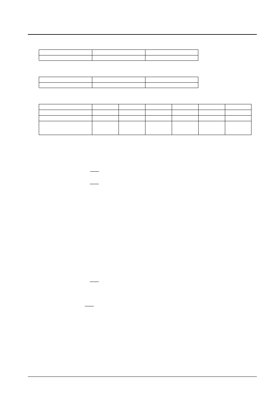
V flag output selection (DI9)
Source selection (DI10)
Audio data output format setting (DI11, DI12, DI13)
DI4 to DI13 are set to an initial value of low, immediately after the XMODE pin goes from low to high. Since DI0
to DI3 and DI14 to DI15 are unused they can be set to either low or high.
Output
C bits
— This product only supports 32 bits, since it is designed for mode 0 consumer applications.
— In readout when CCB/SUB is low, after the output address is loaded into SWDT, the flag (fixed at the high
level) is output on the fall of XLAT, and then 32 bits of data is output according to SCLK.
— In readout when CCB/SUB is high, after the output address is loaded into DI, the 32 bits of data are output
from DO according to CL while CE is high.
— Since the C bits are not checked for errors, processing is performed after the PLL lock state is detected.
Therefore, data must be read out only after the ERROR pin goes low.
— If a lock error occurs during readout (ERROR = high), the shift register will be reset and all data will become 0
(low). However, while the ERROR pin will also go high on a parity error, this error processing will not be
performed.
— An interval of at least 6 ms or longer must be provided between readout operations.
Subcode Q
— The LC8904Q provides the following two functions for subcode readout:
1. CD subcode interface (CP-2401) is possible
2. Output of subcode Q data with CRC flags included, which corresponds to the CD and MD formats
The microprocessor interface uses the readout function of item 2.
— The subcode Q data, which is reproduced at 1 bit per frame, is input to an 80-bit register and a CRC checking
circuit. After the 96 bits of data have been input, it is loaded into a shift register on the falling edge of
LD/DQSY. The data must be read out after this load operation.
— In readout when CCB/SUB is low, after the output address has been loaded into SWDT, the CRC flags are
output on the falling edge of XLAT. If the CRC flags indicate that the check was OK, a high level is output.
Next, 80 bits of data is output from SRDT according to SCLK. Note that the subcode Q data is updated on
every falling edge of the DQSY signal.
— Readout when CCB/SUB is high is identical to that described in item 3. (See the timing charts for details.)
— The data output from SRDT (DO) has the same order on a per-byte basis, but the bit order within each byte is
LSB first.
— If a lock error occurs between the fall of DQSY and the fall of XLAT, the CRC flags will go low. However, if
a lock error after the fall of XLAT, the CRC flags will not go low, since correct data will be output.
No. 5014-14/20
LC8904Q
DI9
L
H
DOUT/V pin
Data selected by DI7 and DI8
V flag
DI10
L
H
Mode
Digital source
Analog source
DI11
L
H
DI12
L
H
L
H
DI13
L
H
L
H
16 bits
20 bits
DATAOUT
MSB first
LSB first
MSB first
LSB first
Rear packed
Front packed
Rear packed
Front packed
相关PDF资料 |
PDF描述 |
|---|---|
| LC89051V | SPECIALTY CONSUMER CIRCUIT, PDSO24 |
| LC89052TA-E | SPECIALTY CONSUMER CIRCUIT, PDSO24 |
| LC890561W | SPECIALTY CONSUMER CIRCUIT, PQFP48 |
| LC890561W | SPECIALTY CONSUMER CIRCUIT, PQFP48 |
| LC89057W-VF4-E | SPECIALTY CONSUMER CIRCUIT, PQFP48 |
相关代理商/技术参数 |
参数描述 |
|---|---|
| LC89051V | 制造商:SANYO 制造商全称:Sanyo Semicon Device 功能描述:Digital Audio Interface Receiver |
| LC89052T | 制造商:SANYO 制造商全称:Sanyo Semicon Device 功能描述:Digital Audio Interface Receiver |
| LC89052TA-E | 功能描述:音频发送器、接收器、收发器 RoHS:否 制造商:Cirrus Logic 工作电源电压:3.3 V, 5 V 电源电流:11.8 mA 通道数量:1 最大工作温度:+ 70 C 接口类型:I2C, SPI 安装风格:SMD/SMT 封装 / 箱体:TSSOP-28 封装: |
| LC89052TA-TLM-E | 功能描述:音频发送器、接收器、收发器 RoHS:否 制造商:Cirrus Logic 工作电源电压:3.3 V, 5 V 电源电流:11.8 mA 通道数量:1 最大工作温度:+ 70 C 接口类型:I2C, SPI 安装风格:SMD/SMT 封装 / 箱体:TSSOP-28 封装: |
| LC89052THS-E | 制造商:ON Semiconductor 功能描述:AUDIO I/F RECEIVER |
发布紧急采购,3分钟左右您将得到回复。