- 您现在的位置:买卖IC网 > PDF目录19862 > LCMXO1200C-3TN100C (Lattice Semiconductor Corporation)IC PLD 1200LUTS 73I/O 100-TQFP PDF资料下载
参数资料
| 型号: | LCMXO1200C-3TN100C |
| 厂商: | Lattice Semiconductor Corporation |
| 文件页数: | 44/88页 |
| 文件大小: | 0K |
| 描述: | IC PLD 1200LUTS 73I/O 100-TQFP |
| 标准包装: | 90 |
| 系列: | MachXO |
| 可编程类型: | 系统内可编程 |
| 最大延迟时间 tpd(1): | 5.1ns |
| 电压电源 - 内部: | 1.71 V ~ 3.465 V |
| 宏单元数: | 600 |
| 输入/输出数: | 73 |
| 工作温度: | 0°C ~ 85°C |
| 安装类型: | 表面贴装 |
| 封装/外壳: | 100-LQFP |
| 供应商设备封装: | 100-TQFP(14x14) |
| 包装: | 托盘 |
| 其它名称: | 220-1177 |
第1页第2页第3页第4页第5页第6页第7页第8页第9页第10页第11页第12页第13页第14页第15页第16页第17页第18页第19页第20页第21页第22页第23页第24页第25页第26页第27页第28页第29页第30页第31页第32页第33页第34页第35页第36页第37页第38页第39页第40页第41页第42页第43页当前第44页第45页第46页第47页第48页第49页第50页第51页第52页第53页第54页第55页第56页第57页第58页第59页第60页第61页第62页第63页第64页第65页第66页第67页第68页第69页第70页第71页第72页第73页第74页第75页第76页第77页第78页第79页第80页第81页第82页第83页第84页第85页第86页第87页第88页
�� �
�
�MachXO� Family� Data� Sheet�
�Pinout� Information�
�November� 2012�
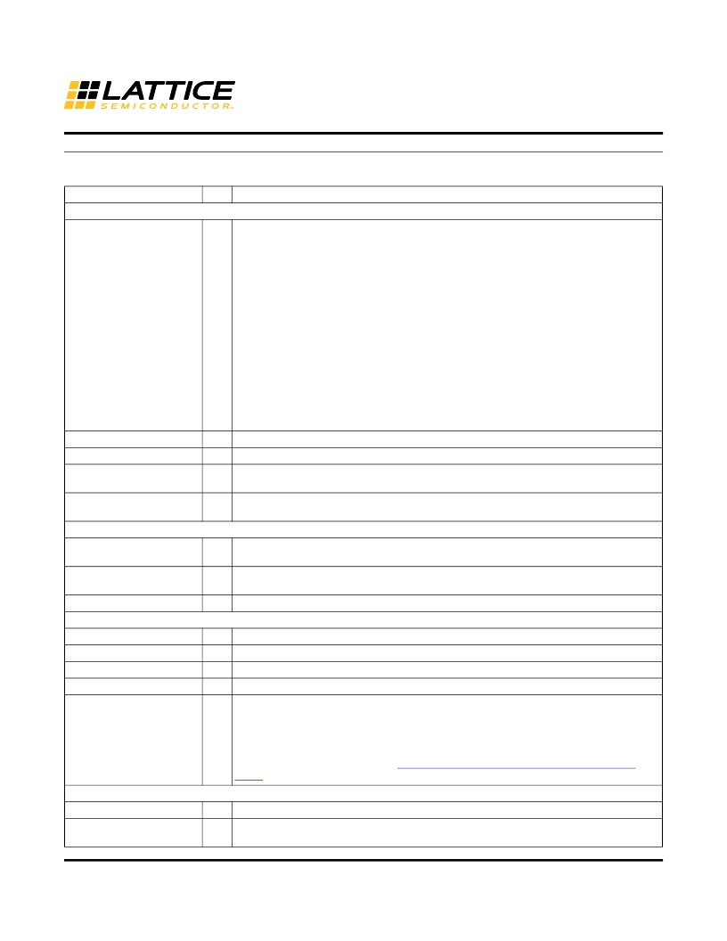
�Signal� Descriptions�
�Data� Sheet� DS1002�
�Signal� Name�
�I/O�
�Descriptions�
�General� Purpose�
�[Edge]� indicates� the� edge� of� the� device� on� which� the� pad� is� located.� Valid� edge� designa-�
�tions� are� L� (Left),� B� (Bottom),� R� (Right),� T� (Top).�
�[Row/Column� Number]� indicates� the� PFU� row� or� the� column� of� the� device� on� which� the�
�PIO� Group� exists.� When� Edge� is� T� (Top)� or� (Bottom),� only� need� to� specify� Row� Number.�
�When� Edge� is� L� (Left)� or� R� (Right),� only� need� to� specify� Column� Number.�
�[A/B/C/D]� indicates� the� PIO� within� the� group� to� which� the� pad� is� connected.�
�P[Edge]� [Row/Column�
�Number]_[A/B/C/D]�
�I/O� Some� of� these� user-programmable� pins� are� shared� with� special� function� pins.� When� not�
�used� as� special� function� pins,� these� pins� can� be� programmed� as� I/Os� for� user� logic.�
�During� configuration� of� the� user-programmable� I/Os,� the� user� has� an� option� to� tri-state� the� ?�
�I/Os� and� enable� an� internal� pull-up,� pull-down� or� buskeeper� resistor.� This� option� also�
�applies� to� unused� pins� (or� those� not� bonded� to� a� package� pin).� The� default� during� configu-�
�ration� is� for� user-programmable� I/Os� to� be� tri-stated� with� an� internal� pull-down� resistor�
�enabled.� When� the� device� is� erased,� I/Os� will� be� tri-stated� with� an� internal� pull-down� resis-�
�tor� enabled.� Some� pins,� such� as� PROGRAMN� and� JTAG� pins,� default� to� tri-stated� I/Os� with�
�pull-up� resistors� enabled� when� the� device� is� erased.�
�NC�
�GND�
�VCC�
�VCCIOx�
�—�
�—�
�—�
�—�
�No� connect.�
�GND� –� Ground.� Dedicated� pins.� It� is� recommended� that� all� GNDs� are� tied� together.�
�V� CC� –� The� power� supply� pins� for� core� logic.� Dedicated� pins.� It� is� recommended� that� all�
�VCCs� are� tied� to� the� same� supply.�
�VCCIO� –� The� power� supply� pins� for� I/O� Bank� x.� Dedicated� pins.� It� is� recommended� that� all�
�VCCIOs� located� in� the� same� bank� are� tied� to� the� same� supply.�
�PLL� and� Clock� Functions� (Used� as� user-programmable� I/O� pins� when� not� used� for� PLL� or� clock� pins)�
�[LOC]_GPLL[T,� C]_IN�
�[LOC]_GPLL[T,� C]_FB�
�PCLK� [n]_[2:0]�
�—�
�—�
�—�
�Reference� Clock� (PLL)� input� pads:� [LOC]� indicates� location.� Valid� designations� are� L� (Left�
�PLL)� and� R� (Right� PLL).� T� =� true� and� C� =� complement.�
�Optional� Feedback� (PLL)� input� pads:� [LOC]� indicates� location.� Valid� designations� are� L�
�(Left� PLL)� and� R� (Right� PLL).� T� =� true� and� C� =� complement.�
�Primary� Clock� pads.� One� to� three� clock� pads� per� side.�
�Test� and� Programming� (Dual� function� pins� used� for� test� access� port� and� during� sysCONFIG?)�
�TMS�
�TCK�
�TDI�
�TDO�
�JTAGENB�
�I�
�I�
�I�
�O�
�I�
�Test� Mode� Select� input� pin,� used� to� control� the� 1149.1� state� machine.�
�Test� Clock� input� pin,� used� to� clock� the� 1149.1� state� machine.�
�Test� Data� input� pin,� used� to� load� data� into� the� device� using� an� 1149.1� state� machine.�
�Output� pin� –� Test� Data� output� pin� used� to� shift� data� out� of� the� device� using� 1149.1.�
�Optionally� controls� behavior� of� TDI,� TDO,� TMS,� TCK.� If� the� device� is� configured� to� use� the�
�JTAG� pins� (TDI,� TDO,� TMS,� TCK)� as� general� purpose� I/O,� then:�
�If� JTAGENB� is� low:� TDI,� TDO,� TMS� and� TCK� can� function� a� general� purpose� I/O.�
�If� JTAGENB� is� high:� TDI,� TDO,� TMS� and� TCK� function� as� JTAG� pins.�
�For� more� details,� refer� to� TN1204,� MachXO2 Programming and Configuration Usage�
��Configuration� (Dual� function� pins� used� during� sysCONFIG)�
�PROGRAMN�
�INITN�
�I�
�I/O�
�Initiates� configuration� sequence� when� asserted� low.� This� pin� always� has� an� active� pull-up.�
�Open� Drain� pin.� Indicates� the� FPGA� is� ready� to� be� configured.� During� configuration,� a� pull-�
�up� is� enabled.�
�?� 2012� Lattice� Semiconductor� Corp.� All� Lattice� trademarks,� registered� trademarks,� patents,� and� disclaimers� are� as� listed� at� www.latticesemi.com/legal.� All� other� brand�
�or� product� names� are� trademarks� or� registered� trademarks� of� their� respective� holders.� The� specifications� and� information� herein� are� subject� to� change� without� notice.�
�www.latticesemi.com�
�4-1�
�DS1002� Pinouts_01.9�
�相关PDF资料 |
PDF描述 |
|---|---|
| HMC30DRXS | CONN EDGECARD 60POS DIP .100 SLD |
| GBB45DHBR | CONN EDGECARD 90POS R/A .050 SLD |
| V110C12H100BF3 | CONVERTER MOD DC/DC 12V 100W |
| GBM18DRMD-S288 | CONN EDGECARD 36POS .156 EXTEND |
| AYM22DRSN-S664 | CONN EDGECARD 44POS DIP .156 SLD |
相关代理商/技术参数 |
参数描述 |
|---|---|
| LCMXO1200C-3TN100I | 功能描述:CPLD - 复杂可编程逻辑器件 1200 LUTs 73 I/O 1.8/2.5/3.3V IND RoHS:否 制造商:Lattice 系列: 存储类型:EEPROM 大电池数量:128 最大工作频率:333 MHz 延迟时间:2.7 ns 可编程输入/输出端数量:64 工作电源电压:3.3 V 最大工作温度:+ 90 C 最小工作温度:0 C 封装 / 箱体:TQFP-100 |
| LCMXO1200C-3TN144C | 功能描述:CPLD - 复杂可编程逻辑器件 1200 LUTS 113 I/O RoHS:否 制造商:Lattice 系列: 存储类型:EEPROM 大电池数量:128 最大工作频率:333 MHz 延迟时间:2.7 ns 可编程输入/输出端数量:64 工作电源电压:3.3 V 最大工作温度:+ 90 C 最小工作温度:0 C 封装 / 箱体:TQFP-100 |
| LCMXO1200C-3TN144I | 功能描述:CPLD - 复杂可编程逻辑器件 1200 LUTs 113 IO 1.8 /2.5/3.3V -3 Spd I RoHS:否 制造商:Lattice 系列: 存储类型:EEPROM 大电池数量:128 最大工作频率:333 MHz 延迟时间:2.7 ns 可编程输入/输出端数量:64 工作电源电压:3.3 V 最大工作温度:+ 90 C 最小工作温度:0 C 封装 / 箱体:TQFP-100 |
| LCMXO1200C-4B256C | 功能描述:CPLD - 复杂可编程逻辑器件 1200 LUTs 211 I/O 1.8/2.5/3.3V -4 SPD RoHS:否 制造商:Lattice 系列: 存储类型:EEPROM 大电池数量:128 最大工作频率:333 MHz 延迟时间:2.7 ns 可编程输入/输出端数量:64 工作电源电压:3.3 V 最大工作温度:+ 90 C 最小工作温度:0 C 封装 / 箱体:TQFP-100 |
| LCMXO1200C-4B256I | 功能描述:CPLD - 复杂可编程逻辑器件 1200 LUTs 211 I/O 1.8/2.5/3.3V -4 SPD RoHS:否 制造商:Lattice 系列: 存储类型:EEPROM 大电池数量:128 最大工作频率:333 MHz 延迟时间:2.7 ns 可编程输入/输出端数量:64 工作电源电压:3.3 V 最大工作温度:+ 90 C 最小工作温度:0 C 封装 / 箱体:TQFP-100 |
发布紧急采购,3分钟左右您将得到回复。