- 您现在的位置:买卖IC网 > PDF目录44530 > LM1572MTCX-3.3/NOPB (NATIONAL SEMICONDUCTOR CORP) 3.2 A SWITCHING REGULATOR, 570 kHz SWITCHING FREQ-MAX, PDSO16 PDF资料下载
参数资料
| 型号: | LM1572MTCX-3.3/NOPB |
| 厂商: | NATIONAL SEMICONDUCTOR CORP |
| 元件分类: | 稳压器 |
| 英文描述: | 3.2 A SWITCHING REGULATOR, 570 kHz SWITCHING FREQ-MAX, PDSO16 |
| 封装: | TSSOP-16 |
| 文件页数: | 17/17页 |
| 文件大小: | 583K |
| 代理商: | LM1572MTCX-3.3/NOPB |
Application Information
Resistive Divider Calculation
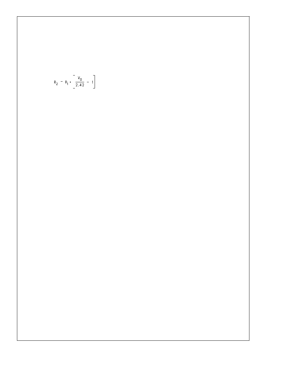
For the adjustable part, the voltage on the feedback pin is set
to 2.42V under regulation. This is achieved by means of a
resistive divider, as indicated in the Typical Applications for
the adjustable part. Designating the upper resistor as ’R
2’
(connected to the output) and the lower resistor as ’R
1’
(connected to ground), the following equation relates R
1,R2
and the output voltage level V
O :
Setting the lower resistor to 2.21k (which is a standard
resistance value), the upper resistor is chosen as 806 ohms
for a 3.3V output and as 2.37k for a 5V output. This should
suffice for most applications. However the more experienced
designer may like to know more about the rather overlooked
intricacy of selecting resistors especially in regard to the
resultant error in the output voltage. It is also helpful to
consider the other factors affecting the tolerance of the
output voltage. This is disussed under ’Tolerance of set
Output Voltage’ at the end of ’Application Information’. Note
that if the the lower resistor is set to 2.21k, the divider current
is greater than 1mA, so a 0.1F boostrap will always suffice
(see Pin Descriptions for Pin 1 and Pin 15 above).
Inductor Selection
Inductor selection for buck converters is discussed in great
detail in AN-1197, to which the reader can refer to for a
deeper understanding. It must be understood that though the
scope of the above Application Note is limited to buck con-
verters that rely on voltage mode control, all the consider-
ations contained therein also apply to buck converters rely-
ing on current mode control, such as the LM1572. In fact,
with current mode control, there are additional consider-
ations that may apply which need to be discussed here.
The basic requirement for any converter is that it should be
able to deliver the required power without hitting the current
limit of the switch. This is ensured by having an inductance
large enough to limit the peak current (this is obviously not
feasible if the required load current is very close to or larger
than the current limit!). In the LM1572, a ’slope compensa-
tion’ ramp is also summed-in with the switch current ramp,
for duty cycles greater than 0.5. The reason for this slope
compensation will be explained later below, here it suffices
to realize that it affects the effective current limit for duty
cycles greater than 0.5. From the Electrical Characteristics it
can be seen that the current limit I
CLIM is stated as two
terms: one for D less than (or equal to) 0.5, and one for D =
0.8. Since the current limit falls off at high duty cycles/low
input voltage due to the slope compensation, a peak power
calculation should generally be done both at the highest and
the lowest input voltage, so as to ensure that the inductance
is large enough to cover the entire desired operating input
voltage range.
The overall strategy here is to determine various ’minimum
inductances’ based on all different considerations (as appli-
cable), and to then pick the largest of all the ’minimums’ so
as to satisfy each of the conditions.
It is noted here that there can also be an ’optimum’ value for
the inductance, one which offers a compromise solution for
reducing the overall size of the power converter, the mag-
netics and capacitors included. However, since the primary
reason for going to higher switching frequencies is to reduce
the size of the magnetics alone, ’optimization’ may be rel-
egated to a lower priority, as in the example to follow.
In (peak) current mode control, the main additional consid-
eration is the phenomenon of subharmonic instability (also
called alternate cycle or half-frequency oscillations). This is
fundamental to the topology, and no amount of ’tweaking’ the
compensation resistor/capacitor values will circumvent it.
The well known solution is to add a certain amount of ’slope
compensation’, the value of which is directly related to the
inductance being used. Higher inductance requires smaller
slope compensation. If the slope compensation is fixed, as
for the LM1572, it is the inductance that needs to be con-
trolled. Then higher slope compensation requires smaller
inductance. This defines a ’minimum’ value of inductance
required to avoid subharmonic instability. The value can
therefore be exceeded. If for example the first priority in a
given application is not the size of the inductor, but the
reduction of output ripple, a higher than the minimum induc-
tance may be selected. But too high an inductance, for a
given slope compensation (or equivalently too much of slope
compensation for a given inductance), will cause the loop
response to become more and more that of voltage mode
control, eventually making it slower and harder to compen-
sate. For any LM1572 design therefore, the maximum rec-
ommended inductance is 15H, irrespective of input or out-
put conditions.
For the LM1572, the slope compensation can vary (from
device to device) over the range 0.42 to 0.75 A/s. A little
thought will lead to the conclusion that any calculation for the
minimum inductance (required to avoid subharmonic insta-
bility), must be carried out at its ’worst-case’: which is the
lower limit of the slope compensation (i.e. 0.42 A/s). This
also happens to be the value used for peak power calcula-
tion since it corresponds to the lower limit of current limit
(2A). The value of 0.75 A/s can be used to check if the
slope compensation is not ’excessive’ in the sense dis-
cussed above.
The effective current limit, ’I
CLIM’ (see Electrical Characteris-
tics) is the sum of two terms. The first is the basic preset
current limit (the flat part) , which we call ’I
CL’ here, and is the
value given for ’I
CLIM’ for D
≤ 0.5). Superimposed on this is
the effect of slope compensation. This causes the current
limit to fall (almost linearly) for D > 0.5. In general, the slope
compensation can be expressed as ’m
C’ in units of A/s.
From D = 0.5 to a projected value of D = 1 (a time interval of
1s), the current limit would therefore fall exactly by m
C
Amps. At D = 0.8 the current limit falls by 3/5th of this i.e. by
m
C*0.6. So the current limit at D = 0.8 would be ICL
(0.6*m
C). This value (’ICLIM’ for D = 0.8 ) is also given in the
Electrical Characteristics tables.
As mentioned, the inductance must be chosen to be higher
than the minimum value corresponding to the condition of
peak calculated switch current equal to the current limit. The
worst case must be used here: i.e. the ’min’ of current limit
values in the Electrical Characteristics (not ’typ’). Further, it
should be confirmed over the entire input voltage range (or
duty cycle) that the peak current does not attempt to exceed
the effective current limit. This is easily carried out using the
same general strategy: by calculating the minimum induc-
tance at both input voltage extremes, and then choosing the
greater of the two calculated ’minimum’ inductances.
It should also be remembered that subharmonic instability
can only occur when several conditions are simultaneously
satisfied: (peak) current mode control, duty cycle greater
than (or around) 0.5, and continuous conduction mode. Sub-
LM1572
www.national.com
9
相关PDF资料 |
PDF描述 |
|---|---|
| LM1572MTC-3.3/NOPB | 3.2 A SWITCHING REGULATOR, 570 kHz SWITCHING FREQ-MAX, PDSO16 |
| LM1572MTC-ADJ/NOPB | 3.2 A SWITCHING REGULATOR, 570 kHz SWITCHING FREQ-MAX, PDSO16 |
| LM1575J-ADJ/883 | 3 A SWITCHING REGULATOR, 58 kHz SWITCHING FREQ-MAX, CDIP16 |
| LM1575J-5.0/883 | 3 A SWITCHING REGULATOR, 58 kHz SWITCHING FREQ-MAX, CDIP16 |
| LM1575J-15/883 | 3 A SWITCHING REGULATOR, 58 kHz SWITCHING FREQ-MAX, CDIP16 |
相关代理商/技术参数 |
参数描述 |
|---|---|
| LM1572MTCX-5.0/NOPB | 功能描述:IC REG BUCK 5V 1.5A 16TSSOP RoHS:是 类别:集成电路 (IC) >> PMIC - 稳压器 - DC DC 开关稳压器 系列:- 产品培训模块:Lead (SnPb) Finish for COTS Obsolescence Mitigation Program 标准包装:1 系列:- 类型:降压(降压) 输出类型:固定 输出数:1 输出电压:3.3V 输入电压:4.5 V ~ 24 V PWM 型:- 频率 - 开关:- 电流 - 输出:125mA 同步整流器:无 工作温度:-40°C ~ 85°C 安装类型:表面贴装 封装/外壳:SOT-23-6 包装:Digi-Reel® 供应商设备封装:SOT-6 其它名称:MAX1836EUT33#TG16DKR |
| LM1572MTCX-ADJ/NOPB | 功能描述:IC REG BUCK ADJ 1.5A 16TSSOP RoHS:是 类别:集成电路 (IC) >> PMIC - 稳压器 - DC DC 开关稳压器 系列:- 产品培训模块:Lead (SnPb) Finish for COTS Obsolescence Mitigation Program 标准包装:1 系列:- 类型:降压(降压) 输出类型:固定 输出数:1 输出电压:3.3V 输入电压:4.5 V ~ 24 V PWM 型:- 频率 - 开关:- 电流 - 输出:125mA 同步整流器:无 工作温度:-40°C ~ 85°C 安装类型:表面贴装 封装/外壳:SOT-23-6 包装:Digi-Reel® 供应商设备封装:SOT-6 其它名称:MAX1836EUT33#TG16DKR |
| LM1575 | 制造商:NSC 制造商全称:National Semiconductor 功能描述:SIMPLE SWITCHER㈢ 1A Step-Down Voltage Regulator |
| LM1575_07 | 制造商:NSC 制造商全称:National Semiconductor 功能描述:SIMPLE SWITCHER㈢ 1A Step-Down Voltage Regulator |
| LM1575-12 | 制造商:NSC 制造商全称:National Semiconductor 功能描述:SIMPLE SWITCHER 1A STEP-DOWN VOLTAGE REGULATOR |
发布紧急采购,3分钟左右您将得到回复。