- 您现在的位置:买卖IC网 > PDF目录240272 > LM1575-5.0MD8 (NATIONAL SEMICONDUCTOR CORP) 3.2 A SWITCHING REGULATOR, 62 kHz SWITCHING FREQ-MAX, UUC PDF资料下载
参数资料
| 型号: | LM1575-5.0MD8 |
| 厂商: | NATIONAL SEMICONDUCTOR CORP |
| 元件分类: | 稳压器 |
| 英文描述: | 3.2 A SWITCHING REGULATOR, 62 kHz SWITCHING FREQ-MAX, UUC |
| 封装: | DIE |
| 文件页数: | 10/40页 |
| 文件大小: | 917K |
| 代理商: | LM1575-5.0MD8 |
第1页第2页第3页第4页第5页第6页第7页第8页第9页当前第10页第11页第12页第13页第14页第15页第16页第17页第18页第19页第20页第21页第22页第23页第24页第25页第26页第27页第28页第29页第30页第31页第32页第33页第34页第35页第36页第37页第38页第39页第40页
Application Hints (Continued)
Since the lead frame is solid copper, heat from the die is
readily conducted through the leads to the printed circuit
board copper, which is acting as a heat sink.
For best thermal performance, the ground pins and all the
unconnected pins should be soldered to generous amounts
of printed circuit board copper, such as a ground plane.
Large areas of copper provide the best transfer of heat to the
surrounding air. Copper on both sides of the board is also
helpful in getting the heat away from the package, even if
there is no direct copper contact between the two sides.
Thermal resistance numbers as low as 40C/W for the SO
package, and 30C/W for the N package can be realized with
a carefully engineered pc board.
Included on the
Switchers Made Simple design software is
a more precise (non-linear) thermal model that can be used
to determine junction temperature with different input-output
parameters or different component values. It can also calcu-
late the heat sink thermal resistance required to maintain the
regulators junction temperature below the maximum operat-
ing temperature.
Additional Applications
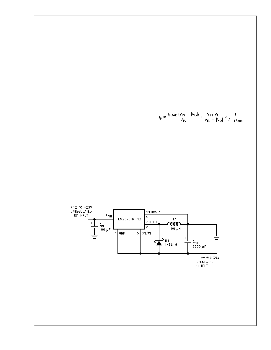
INVERTING REGULATOR
Figure 10 shows a LM2575-12 in a buck-boost configuration
to generate a negative 12V output from a positive input
voltage. This circuit bootstraps the regulator’s ground pin to
the negative output voltage, then by grounding the feedback
pin, the regulator senses the inverted output voltage and
regulates it to 12V.
For an input voltage of 12V or more, the maximum available
output current in this configuration is approximately 0.35A. At
lighter loads, the minimum input voltage required drops to
approximately 4.7V.
The switch currents in this buck-boost configuration are
higher than in the standard buck-mode design, thus lowering
the available output current. Also, the start-up input current
of the buck-boost converter is higher than the standard
buck-mode regulator, and this may overload an input power
source with a current limit less than 1.5A. Using a delayed
turn-on or an undervoltage lockout circuit (described in the
next section) would allow the input voltage to rise to a high
enough level before the switcher would be allowed to turn
on.
Because of the structural differences between the buck and
the buck-boost regulator topologies, the buck regulator de-
sign procedure section can not be used to to select the
inductor or the output capacitor. The recommended range of
inductor values for the buck-boost design is between 68 H
and 220 H, and the output capacitor values must be larger
than what is normally required for buck designs. Low input
voltages or high output currents require a large value output
capacitor (in the thousands of micro Farads).
The peak inductor current, which is the same as the peak
switch current, can be calculated from the following formula:
Where f
osc = 52 kHz. Under normal continuous inductor
current operating conditions, the minimum V
IN represents
the worst case. Select an inductor that is rated for the peak
current anticipated.
Also, the maximum voltage appearing across the regulator is
the absolute sum of the input and output voltage. For a 12V
output, the maximum input voltage for the LM2575 is +28V,
or +48V for the LM2575HV.
The
Switchers Made Simple (version 3.3) design software
can be used to determine the feasibility of regulator designs
using different topologies, different input-output parameters,
different components, etc.
NEGATIVE BOOST REGULATOR
Another variation on the buck-boost topology is the negative
boost configuration. The circuit in
Figure 11 accepts an input
voltage ranging from 5V to 12V and provides a regulated
12V output. Input voltages greater than 12V will cause the
output to rise above 12V, but will not damage the regulator.
Because of the boosting function of this type of regulator, the
switch current is relatively high, especially at low input volt-
ages. Output load current limitations are a result of the
maximum current rating of the switch. Also, boost regulators
can not provide current limiting load protection in the event of
a shorted load, so some other means (such as a fuse) may
be necessary.
01147515
FIGURE 10. Inverting Buck-Boost Develops 12V
LM1575/LM2575/LM2575HV
www.national.com
18
相关PDF资料 |
PDF描述 |
|---|---|
| LM4050BIX3-2.5+T | 1-OUTPUT TWO TERM VOLTAGE REFERENCE, 2.5 V, PDSO3 |
| LPC5S | 1-OUTPUT 50 W DC-DC REG PWR SUPPLY MODULE |
| LPC9D | 2-OUTPUT 65 W DC-DC REG PWR SUPPLY MODULE |
| LMB5SP | 1-OUTPUT 50 W DC-DC REG PWR SUPPLY MODULE |
| LM4040BIZ-8.2X | 1-OUTPUT TWO TERM VOLTAGE REFERENCE, 8.192 V, PBCY3 |
相关代理商/技术参数 |
参数描述 |
|---|---|
| LM1575AK | 制造商:未知厂家 制造商全称:未知厂家 功能描述:Voltage-Mode SMPS Controller |
| LM1575HVK-12/883 | 制造商:未知厂家 制造商全称:未知厂家 功能描述:Voltage-Mode SMPS Controller |
| LM1575HVK12/883QF | 制造商:Rochester Electronics LLC 功能描述:- Bulk 制造商:Texas Instruments 功能描述: |
| LM1575HVK-15/883 | 制造商:未知厂家 制造商全称:未知厂家 功能描述:Voltage-Mode SMPS Controller |
| LM1575HVK-3.3/883 | 制造商:未知厂家 制造商全称:未知厂家 功能描述:Voltage-Mode SMPS Controller |
发布紧急采购,3分钟左右您将得到回复。