- 您现在的位置:买卖IC网 > PDF目录178069 > LM2576 (ON SEMICONDUCTOR) 3.0 A, 15 V, Step-Down Switching Regulator(3.0A,15V,降压型开关稳压器) PDF资料下载
参数资料
| 型号: | LM2576 |
| 厂商: | ON SEMICONDUCTOR |
| 英文描述: | 3.0 A, 15 V, Step-Down Switching Regulator(3.0A,15V,降压型开关稳压器) |
| 中文描述: | 3.0甲,15 V的,降压型开关稳压器(3.0A的,15V的,降压型开关稳压器) |
| 文件页数: | 10/28页 |
| 文件大小: | 275K |
| 代理商: | LM2576 |
第1页第2页第3页第4页第5页第6页第7页第8页第9页当前第10页第11页第12页第13页第14页第15页第16页第17页第18页第19页第20页第21页第22页第23页第24页第25页第26页第27页第28页
LM2576
http://onsemi.com
18
beyond approximately 6.0 in2 (4000 mm2) will not improve
heat
dissipation
significantly.
If
further
thermal
improvements are needed, double sided or multilayer PC
boards with large copper areas should be considered. In
order to achieve the best thermal performance, it is highly
recommended to use wide copper traces as well as large
areas of copper in the printed circuit board layout. The only
exception to this is the OUTPUT (switch) pin, which should
not have large areas of copper (see page 8 ‘PCB Layout
Thermal Analysis and Design
The following procedure must be performed to determine
whether or not a heatsink will be required. First determine:
1. PD(max)
maximum regulator power dissipation in the
application.
2. TA(max)
maximum ambient temperature in the
application.
3. TJ(max)
maximum allowed junction temperature
(125
°C for the LM2576). For a conservative
design, the maximum junction temperature
should not exceed 110
°C to assure safe
operation. For every additional +10
°C
temperature rise that the junction must
withstand, the estimated operating lifetime
of the component is halved.
4. RqJC
package thermal resistance junctioncase.
5. RqJA
package thermal resistance junctionambient.
(Refer to Maximum Ratings on page 2 of this data sheet or
The following formula is to calculate the approximate
total power dissipated by the LM2576:
PD = (Vin x IQ) + d x ILoad x Vsat
where d is the duty cycle and for buck converter
d
+
ton
T
+
V
O
V
in
,
IQ
(quiescent current) and Vsat can be found in the
LM2576 data sheet,
Vin
is minimum input voltage applied,
VO
is the regulator output voltage,
ILoad is the load current.
The dynamic switching losses during turnon and
turnoff can be neglected if proper type catch diode is used.
Packages Not on a Heatsink (FreeStanding)
For a freestanding application when no heatsink is used,
the junction temperature can be determined by the following
expression:
TJ = (RqJA) (PD) + TA
where (RqJA)(PD) represents the junction temperature rise
caused by the dissipated power and TA is the maximum
ambient temperature.
Packages on a Heatsink
If the actual operating junction temperature is greater than
the selected safe operating junction temperature determined
in step 3, than a heatsink is required. The junction
temperature will be calculated as follows:
TJ = PD (RqJA + RqCS + RqSA) + TA
where
RqJC is the thermal resistance junctioncase,
RqCS is the thermal resistance caseheatsink,
RqSA is the thermal resistance heatsinkambient.
If the actual operating temperature is greater than the
selected safe operating junction temperature, then a larger
heatsink is required.
Some Aspects That can Influence Thermal Design
It should be noted that the package thermal resistance and
the junction temperature rise numbers are all approximate,
and there are many factors that will affect these numbers,
such as PC board size, shape, thickness, physical position,
location, board temperature, as well as whether the
surrounding air is moving or still.
Other factors are trace width, total printed circuit copper
area, copper thickness, single or doublesided, multilayer
board, the amount of solder on the board or even color of the
traces.
The size, quantity and spacing of other components on the
board can also influence its effectiveness to dissipate the heat.
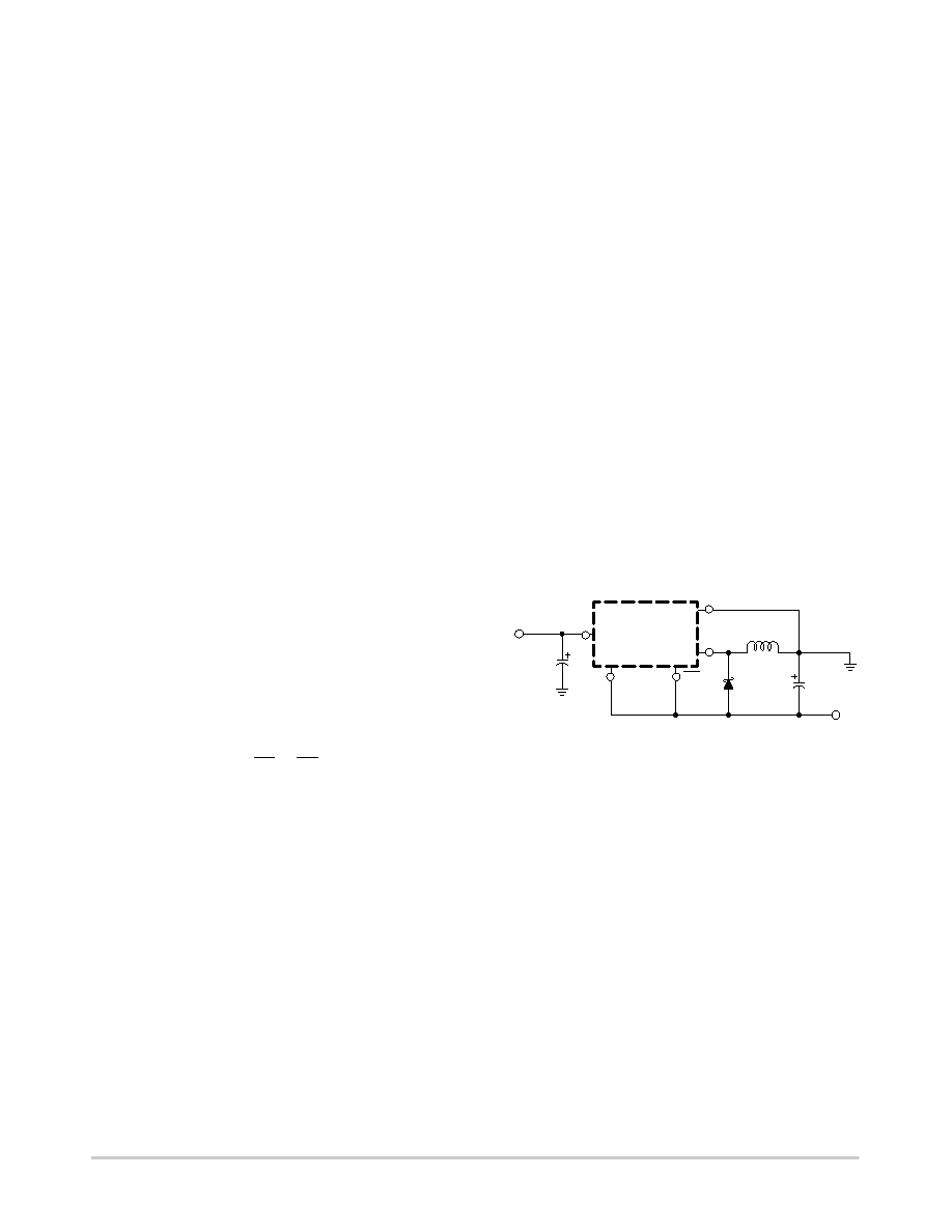
Figure 26. Inverting BuckBoost Develops 12 V
D1
1N5822
L1
68
mH
Output
2
4
Feedback
12 to 40 V
Unregulated
DC Input
Cin
100
mF
1
5
3ON/OFF
GN
D
+Vin
12 V @ 0.7 A
Regulated
Output
Cout
2200
mF
LM257612
ADDITIONAL APPLICATIONS
Inverting Regulator
An inverting buckboost regulator using the LM257612
is shown in Figure 26. This circuit converts a positive input
voltage to a negative output voltage with a common ground
by bootstrapping the regulators ground to the negative
output voltage. By grounding the feedback pin, the regulator
senses the inverted output voltage and regulates it.
In this example the LM257612 is used to generate a
12 V output. The maximum input voltage in this case
cannot exceed +28 V because the maximum voltage
appearing across the regulator is the absolute sum of the
input and output voltages and this must be limited to a
maximum of 40 V.
相关PDF资料 |
PDF描述 |
|---|---|
| LM2742 | N-Channel FET Synchronous Buck Regulator Controller for Low Output Voltages |
| LM2931A | 100 mA, Adjustable Output, LDO Voltage Regulator with 60 V Load Dump Protection(100mA,可调输出,带有60V负载保护的低压差稳压器) |
| LM2931 | 100 mA, Adjustable Output, LDO Voltage Regulator with 60 V Load Dump Protection(100mA,可调输出,带有60V负载保护的低压差稳压器) |
| LM293 | Low Offset Voltage Dual Comparators(低失调电压,2比较器) |
| LM311H | COMPARATOR, 10000 uV OFFSET-MAX, 200 ns RESPONSE TIME, MBCY8 |
相关代理商/技术参数 |
参数描述 |
|---|---|
| LM2576/D | 制造商:未知厂家 制造商全称:未知厂家 功能描述:Easy Switcher? 3.0 A Step-Down Voltage Regulator |
| LM2576_05 | 制造商:MICREL 制造商全称:Micrel Semiconductor 功能描述:52kHz Simple 3A Buck Regulator |
| LM2576_06 | 制造商:ONSEMI 制造商全称:ON Semiconductor 功能描述:3.0 A, 15 V, Step−Down Switching Regulator |
| LM2576_11 | 制造商:HTC 制造商全称:HTC Korea TAEJIN Technology Co. 功能描述:3A, 52kHz, Step-Down Switching Regulator |
| LM2576_12 | 制造商:MOTOROLA 制造商全称:Motorola, Inc 功能描述:EASY SWITCHERER 3.0 A STEPa??DOWN VOLTAGE REGULATOR |
发布紧急采购,3分钟左右您将得到回复。