- 您现在的位置:买卖IC网 > PDF目录44548 > LM2577NADJ (NATIONAL SEMICONDUCTOR CORP) 6 A SWITCHING REGULATOR, 62 kHz SWITCHING FREQ-MAX, PDIP24 PDF资料下载
参数资料
| 型号: | LM2577NADJ |
| 厂商: | NATIONAL SEMICONDUCTOR CORP |
| 元件分类: | 稳压器 |
| 英文描述: | 6 A SWITCHING REGULATOR, 62 kHz SWITCHING FREQ-MAX, PDIP24 |
| 封装: | 0.300 INCH, PLASTIC, DIP-16 |
| 文件页数: | 7/31页 |
| 文件大小: | 1406K |
| 代理商: | LM2577NADJ |
第1页第2页第3页第4页第5页第6页当前第7页第8页第9页第10页第11页第12页第13页第14页第15页第16页第17页第18页第19页第20页第21页第22页第23页第24页第25页第26页第27页第28页第29页第30页第31页
Application Hints (Continued)
STEP-UP (BOOST) REGULATOR
Figure 4 shows the LM1577-ADJ/LM2577-ADJ used as a
Step-Up Regulator. This is a switching regulator used for
producing an output voltage greater than the input supply
voltage.
The
LM1577-12/LM2577-12
and
LM1577-15/
LM2577-15 can also be used for step-up regulators with 12V
or 15V outputs (respectively), by tying the feedback pin
directly to the regulator output.
A basic explanation of how it works is as follows. The
LM1577/LM2577 turns its output switch on and off at a
frequency of 52 kHz, and this creates energy in the inductor
(L). When the NPN switch turns on, the inductor current
charges up at a rate of V
IN/L, storing current in the inductor.
When the switch turns off, the lower end of the inductor flies
above V
IN, discharging its current through diode (D) into the
output capacitor (C
OUT) at a rate of (VOUT VIN)/L. Thus,
energy stored in the inductor during the switch on time is
transferred to the output during the switch off time. The
output voltage is controlled by the amount of energy trans-
ferred which, in turn, is controlled by modulating the peak
inductor current. This is done by feeding back a portion of
the output voltage to the error amp, which amplifies the
difference between the feedback voltage and a 1.230V ref-
erence. The error amp output voltage is compared to a
voltage proportional to the switch current (i.e., inductor cur-
rent during the switch on time).
The comparator terminates the switch on time when the two
voltages are equal, thereby controlling the peak switch cur-
rent to maintain a constant output voltage.
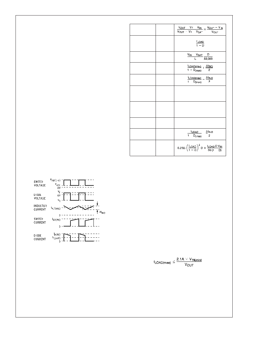
Voltage and current waveforms for this circuit are shown in
Figure 5, and formulas for calculating them are given in
STEP-UP REGULATOR DESIGN PROCEDURE
The following design procedure can be used to select the
appropriate external components for the circuit in Figure 4,
based on these system requirements.
Given:
V
IN (min) = Minimum input supply voltage
V
OUT = Regulated output voltage
I
LOAD(max) = Maximum output load current
Before proceeding any further, determine if the LM1577/
LM2577 can provide these values of V
OUT and ILOAD(max)
when operating with the minimum value of V
IN. The upper
limits for V
OUT and ILOAD(max) are given by the following
equations.
V
OUT
≤ 60V
and
V
OUT
≤ 10xV
IN(min)
These limits must be greater than or equal to the values
specified in this application.
1. Inductor Selection (L)
A. Voltage Options:
1. For 12V or 15V output
output), identify inductor code for region indicated by
V
IN (min)
and I
LOAD (max). The shaded region indicates con-
01146811
FIGURE 5. Step-Up Regulator Waveforms
Duty Cycle
D
Average
Inductor
Current
I
IND(AVE)
Inductor
Current Ripple
I
IND
Peak Inductor
Current
I
IND(PK)
Peak Switch
Current
I
SW(PK)
Switch
Voltage When
Off
V
SW(OFF)
V
OUT +VF
Diode
Reverse
Voltage
V
R
V
OUT VSAT
Average
Diode Current
I
D(AVE)
I
LOAD
Peak Diode
Current
I
D(PK)
Power
Dissipation of
LM1577/2577
P
D
VF = Forward Biased Diode Voltage
ILOAD = Output Load Current
FIGURE 6. Step-Up Regulator Formulas
LM1577/LM2577
www.national.com
15
相关PDF资料 |
PDF描述 |
|---|---|
| LM2577S-15/NOPB | 6 A SWITCHING REGULATOR, 62 kHz SWITCHING FREQ-MAX, PSSO5 |
| LM2577SADJ | 6 A SWITCHING REGULATOR, 62 kHz SWITCHING FREQ-MAX, PSSO5 |
| LM2577S-12X | 6 A SWITCHING REGULATOR, 62 kHz SWITCHING FREQ-MAX, PSSO5 |
| LM2577TADJFLOWLB03 | 6 A SWITCHING REGULATOR, 62 kHz SWITCHING FREQ-MAX, PZFM5 |
| LM2578MWC | 0.75 A SWITCHING REGULATOR, 100 kHz SWITCHING FREQ-MAX, UUC |
相关代理商/技术参数 |
参数描述 |
|---|---|
| LM2577N-ADJ | 功能描述:直流/直流开关转换器 RoHS:否 制造商:STMicroelectronics 最大输入电压:4.5 V 开关频率:1.5 MHz 输出电压:4.6 V 输出电流:250 mA 输出端数量:2 最大工作温度:+ 85 C 安装风格:SMD/SMT |
| LM2577N-ADJ/NOPB | 功能描述:直流/直流开关转换器 RoHS:否 制造商:STMicroelectronics 最大输入电压:4.5 V 开关频率:1.5 MHz 输出电压:4.6 V 输出电流:250 mA 输出端数量:2 最大工作温度:+ 85 C 安装风格:SMD/SMT |
| LM2577S-12 | 功能描述:直流/直流开关转换器 RoHS:否 制造商:STMicroelectronics 最大输入电压:4.5 V 开关频率:1.5 MHz 输出电压:4.6 V 输出电流:250 mA 输出端数量:2 最大工作温度:+ 85 C 安装风格:SMD/SMT |
| LM2577S-12/NOPB | 功能描述:直流/直流开关转换器 RoHS:否 制造商:STMicroelectronics 最大输入电压:4.5 V 开关频率:1.5 MHz 输出电压:4.6 V 输出电流:250 mA 输出端数量:2 最大工作温度:+ 85 C 安装风格:SMD/SMT |
| LM2577S-12/NOPB | 制造商:Texas Instruments 功能描述:DC/DC Converter IC |
发布紧急采购,3分钟左右您将得到回复。