- 您现在的位置:买卖IC网 > PDF目录80008 > LM2592HV3.3MWC (NATIONAL SEMICONDUCTOR CORP) 4 A SWITCHING REGULATOR, 173 kHz SWITCHING FREQ-MAX, UUC PDF资料下载
参数资料
| 型号: | LM2592HV3.3MWC |
| 厂商: | NATIONAL SEMICONDUCTOR CORP |
| 元件分类: | 稳压器 |
| 英文描述: | 4 A SWITCHING REGULATOR, 173 kHz SWITCHING FREQ-MAX, UUC |
| 封装: | WAFER |
| 文件页数: | 18/24页 |
| 文件大小: | 720K |
| 代理商: | LM2592HV3.3MWC |
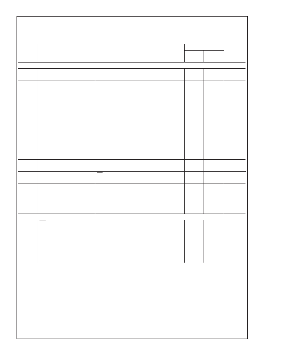
All Output Voltage Versions
Electrical Characteristics
Specifications with standard type face are for T
J = 25C, and those with boldface type apply over full Operating Tempera-
ture Range. Unless otherwise specified, V
IN = 12V for the 3.3V, 5V, and Adjustable version. ILOAD = 500 mA
Symbol
Parameter
Conditions
LM2592HV-XX
Units
(Limits)
Typ
Limit
DEVICE PARAMETERS
I
b
Feedback Bias Current
Adjustable Version Only, V
FB = 1.3V
10
nA
50/100
nA (max)
f
O
Oscillator Frequency
150
kHz
127/110
kHz(min)
173/173
kHz(max)
V
SAT
Saturation Voltage
I
OUT = 2A (Note 7) (Note 8)
1.10
V
1.3/1.4
V(max)
DC
Max Duty Cycle (ON)
100
%
Min Duty Cycle (OFF)
0
I
CLIM
Switch current Limit
Peak Current, (Note 7) (Note 8)
3.0
A
2.4/2.3
A(min)
3.7/4.0
A(max)
I
L
Output Leakage Current
Output = 0V
50
A(max)
Output = 1V
5
mA
30
mA(max)
I
Q
Operating Quiescent
SD /SS Pin Open (Note 9)
5mA
Current
10
mA(max)
I
STBY
Standby Quiescent
SD /SS pin = 0V
90
A
Current
200/250
A(max)
θ
JC
Thermal Resistance
TO220 or TO263 Package, Junction to Case
2
C/W
θ
JA
TO220 Package, Juncton to Ambient (Note 11)
50
C/W
θ
JA
TO263 Package, Juncton to Ambient (Note 12)
50
C/W
θ
JA
TO263 Package, Juncton to Ambient (Note 13)
30
C/W
θ
JA
TO263 Package, Juncton to Ambient (Note 14)
20
C/W
ON/OFF CONTROL Test Circuit
ON /OFF Pin Logic Input
1.3
V
IH
Threshold Voltage
Low (Regulator ON)
0.6
V(max)
V
IL
High (Regulator OFF)
2.0
V(min)
I
H
ON /OFF Pin Input Current
V
LOGIC = 2.5V (Regulator OFF)
5
A
15
A(max)
I
L
V
LOGIC = 0.5V (Regulator ON)
0.02
A
5
A(max)
Note 1: Absolute Maximum Ratings indicate limits beyond which damage to the device may occur. Operating Ratings indicate conditions for which the device is
intended to be functional, but do not guarantee specific performance limits. For guaranteed specifications and test conditions, see the Electrical Characteristics.
Note 2: The human body model is a 100 pF capacitor discharged through a 1.5k resistor into each pin.
Note 3: Typical numbers are at 25C and represent the most likely norm.
Note 4: All limits guaranteed at room temperature (standard type face) and at temperature extremes (bold type face). All room temperature limits are 100%
production tested. All limits at temperature extremes are guaranteed via correlation using standard Statistical Quality Control (SQC) methods. All limits are used
to calculate Average Outgoing Quality Level (AOQL).
Note 5: External components such as the catch diode, inductor, input and output capacitors can affect switching regulator system performance. When the
LM2592HV is used as shown in the
Figure 1 test circuit, system performance will be as shown in system parameters section of Electrical Characteristics.
Note 6: The switching frequency is reduced when the second stage current limit is activated. The amount of reduction is determined by the severity of current
overload.
Note 7: No diode, inductor or capacitor connected to output pin.
Note 8: Feedback pin removed from output and connected to 0V to force the output transistor switch ON.
Note 9: Feedback pin removed from output and connected to 12V for the 3.3V, 5V, and the ADJ. version to force the output transistor switch OFF.
Note 10: VIN = 60V.
LM2592HV
www.national.com
3
相关PDF资料 |
PDF描述 |
|---|---|
| LM3724E2.32MDC | 1-CHANNEL POWER SUPPLY SUPPORT CKT, UUC |
| LT4356HS-1#TR | 1-CHANNEL POWER SUPPLY SUPPORT CKT, PDSO16 |
| LT4356IS-2 | 1-CHANNEL POWER SUPPLY SUPPORT CKT, PDSO16 |
| LMC28SP | 1-OUTPUT 75 W DC-DC REG PWR SUPPLY MODULE |
| LMA5S | 1-OUTPUT 50 W DC-DC REG PWR SUPPLY MODULE |
相关代理商/技术参数 |
参数描述 |
|---|---|
| LM2592HVS-3.3 | 功能描述:直流/直流开关转换器 RoHS:否 制造商:STMicroelectronics 最大输入电压:4.5 V 开关频率:1.5 MHz 输出电压:4.6 V 输出电流:250 mA 输出端数量:2 最大工作温度:+ 85 C 安装风格:SMD/SMT |
| LM2592HVS-3.3/NOPB | 功能描述:直流/直流开关转换器 PWR CONVERTER 150KHz 2A ST-DOWN VLTG REG RoHS:否 制造商:STMicroelectronics 最大输入电压:4.5 V 开关频率:1.5 MHz 输出电压:4.6 V 输出电流:250 mA 输出端数量:2 最大工作温度:+ 85 C 安装风格:SMD/SMT |
| LM2592HVS-5.0 | 功能描述:直流/直流开关转换器 RoHS:否 制造商:STMicroelectronics 最大输入电压:4.5 V 开关频率:1.5 MHz 输出电压:4.6 V 输出电流:250 mA 输出端数量:2 最大工作温度:+ 85 C 安装风格:SMD/SMT |
| LM2592HVS-5.0/NOPB | 功能描述:直流/直流开关转换器 PWR CONVERTER 150KHz 2A ST-DOWN VLTG REG RoHS:否 制造商:STMicroelectronics 最大输入电压:4.5 V 开关频率:1.5 MHz 输出电压:4.6 V 输出电流:250 mA 输出端数量:2 最大工作温度:+ 85 C 安装风格:SMD/SMT |
| LM2592HVS-5.0/NOPB | 制造商:Texas Instruments 功能描述:DC/DC Converter (DC-DC) / Switching Regu |
发布紧急采购,3分钟左右您将得到回复。