- 您现在的位置:买卖IC网 > PDF目录14683 > LM2594DADJR2G (ON Semiconductor)IC REG BUCK ADJ 0.5A 8SOIC PDF资料下载
参数资料
| 型号: | LM2594DADJR2G |
| 厂商: | ON Semiconductor |
| 文件页数: | 19/25页 |
| 文件大小: | 0K |
| 描述: | IC REG BUCK ADJ 0.5A 8SOIC |
| 标准包装: | 2,500 |
| 类型: | 降压(降压) |
| 输出类型: | 可调式 |
| 输出数: | 1 |
| 输出电压: | 1.23 V ~ 37 V |
| 输入电压: | 4.5 V ~ 40 V |
| PWM 型: | 电压模式 |
| 频率 - 开关: | 150kHz |
| 电流 - 输出: | 500mA |
| 同步整流器: | 无 |
| 工作温度: | -40°C ~ 125°C |
| 安装类型: | 表面贴装 |
| 封装/外壳: | 8-SOIC(0.154",3.90mm 宽) |
| 包装: | 带卷 (TR) |
| 供应商设备封装: | 8-SOICN |
| 其它名称: | LM2594DADJR2G-ND LM2594DADJR2GOSTR |
�� �
�
�LM2594�
�+V� in�
�+V� in�
�7�
�LM2594�
�+V�
�0�
�On�
�Off�
�R2�
�Shutdown�
�Input�
�5.0� V�
�0�
�On�
�Off�
�Shutdown�
�Input�
�R3�
�470�
�C� in� R1�
�100� m� F� 47� k�
�5�
�ON/OFF� 6�
�R2�
�GN�
�D�
�+V� in�
�5.6� k�
�C� in�
�100� m� F�
�Q1�
�+V� in�
�7�
�LM2594�
�47� k�
�2N3906�
�5�
�ON/OFF� 6�
�GN�
�-V� out�
�D�
�MOC8101�
�R1�
�12� k�
�-V� out�
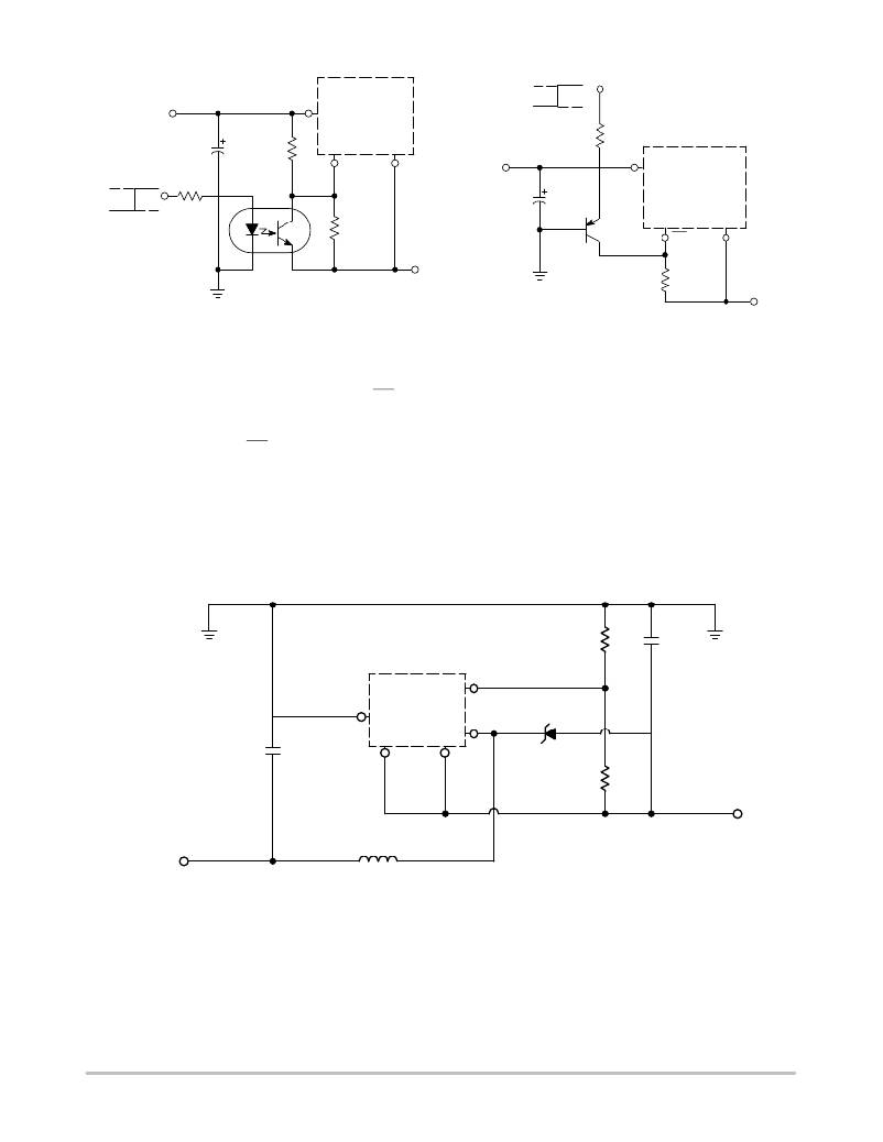
�NOTE:� This� picture� does� not� show� the� complete� circuit.�
�Figure� 25.� Inverting� Buck� ?� Boost� Regulator� Shutdown�
�Circuit� Using� an� Optocoupler�
�With� the� inverting� configuration,� the� use� of� the� ON/OFF�
�pin� requires� some� level� shifting� techniques.� This� is� caused�
�by� the� fact,� that� the� ground� pin� of� the� converter� IC� is� no�
�longer� at� ground.� Now,� the� ON/OFF� pin� threshold� voltage�
�(1.3� V� approximately)� has� to� be� related� to� the� negative�
�output� voltage� level.� There� are� many� different� possible� shut�
�down� methods,� two� of� them� are� shown� in� Figures� 25� and� 26.�
�NOTE:� This� picture� does� not� show� the� complete� circuit.�
�Figure� 26.� Inverting� Buck� ?� Boost� Regulator� Shutdown�
�Circuit� Using� a� PNP� Transistor�
�Negative� Boost� Regulator�
�This� example� is� a� variation� of� the� buck� ?� boost� topology�
�and� it� is� called� negative� boost� regulator.� This� regulator�
�experiences� relatively� high� switch� current,� especially� at� low�
�input� voltages.� The� internal� switch� current� limiting� results�
�in� lower� output� load� current� capability.�
�The� circuit� in� Figure� 27� shows� the� negative� boost�
�configuration.� The� input� voltage� in� this� application� ranges�
�from� ?� 5.0� V� to� ?� 12� V� and� provides� a� regulated� ?� 12� V� output.�
�If� the� input� voltage� is� greater� than� ?� 12� V,� the� output� will� rise�
�above� ?� 12� V� accordingly,� but� will� not� damage� the� regulator.�
�R4�
�Feedback�
�C� out�
�470� m� F�
�+V� in�
�LM2594�
�C� in�
�100� m� F/�
�50� V�
�ON/OFF�
�GND�
�D1�
�1N5822�
�R3�
�?� 12� V� @� 0.25� A�
�Regulated�
�Output�
�?� 12� V�
�Unregulated�
�DC� Input�
�L1�
�100� m� H�
�Figure� 27.� Negative� Boost� Regulator�
�Design� Recommendations:�
�The� same� design� rules� as� for� the� previous� inverting�
�buck� ?� boost� converter� can� be� applied.� The� output� capacitor�
�C� out� must� be� chosen� larger� than� would� be� required� for� a� what�
�standard� buck� converter.� Low� input� voltages� or� high� output�
�currents� require� a� large� value� output� capacitor� (in� the� range�
�of� thousands� of� m� F).� The� recommended� range� of� inductor�
�values� for� the� negative� boost� regulator� is� the� same� as� for�
�inverting� converter� design.�
�Another� important� point� is� that� these� negative� boost�
�converters� cannot� provide� current� limiting� load� protection� in�
�the� event� of� a� short� in� the� output� so� some� other� means,� such�
�as� a� fuse,� may� be� necessary� to� provide� the� load� protection.�
�http://onsemi.com�
�19�
�相关PDF资料 |
PDF描述 |
|---|---|
| RMC15DRES-S13 | CONN EDGECARD 30POS .100 EXTEND |
| MC33063AVDR2G | IC REG BUCK BOOST INV ADJ 8SOIC |
| GEC50DRYN-S13 | CONN EDGECARD 100POS .100 EXTEND |
| GEC50DRYH-S13 | CONN EDGECARD 100POS .100 EXTEND |
| GSC15DRTS-S13 | CONN EDGECARD 30POS .100 EXTEND |
相关代理商/技术参数 |
参数描述 |
|---|---|
| LM2594HVM-12 | 功能描述:直流/直流开关转换器 RoHS:否 制造商:STMicroelectronics 最大输入电压:4.5 V 开关频率:1.5 MHz 输出电压:4.6 V 输出电流:250 mA 输出端数量:2 最大工作温度:+ 85 C 安装风格:SMD/SMT |
| LM2594HVM-12/NOPB | 功能描述:直流/直流开关转换器 150KHZ 0.5A STEP- DOWN VLTG REG RoHS:否 制造商:STMicroelectronics 最大输入电压:4.5 V 开关频率:1.5 MHz 输出电压:4.6 V 输出电流:250 mA 输出端数量:2 最大工作温度:+ 85 C 安装风格:SMD/SMT |
| LM2594HVM-12/NOPB | 制造商:Texas Instruments 功能描述:DC/DC Converter (DC-DC) / Switching Regu |
| LM2594HVM-3.3 | 功能描述:直流/直流开关转换器 RoHS:否 制造商:STMicroelectronics 最大输入电压:4.5 V 开关频率:1.5 MHz 输出电压:4.6 V 输出电流:250 mA 输出端数量:2 最大工作温度:+ 85 C 安装风格:SMD/SMT |
| LM2594HVM-3.3/NOPB | 功能描述:直流/直流开关转换器 150KHZ 0.5A STEP- DOWN VLTG REG RoHS:否 制造商:STMicroelectronics 最大输入电压:4.5 V 开关频率:1.5 MHz 输出电压:4.6 V 输出电流:250 mA 输出端数量:2 最大工作温度:+ 85 C 安装风格:SMD/SMT |
发布紧急采购,3分钟左右您将得到回复。