- 您现在的位置:买卖IC网 > PDF目录14440 > LM2596TVADJG (ON Semiconductor)IC REG BUCK ADJ 3A TO220-5 PDF资料下载
参数资料
| 型号: | LM2596TVADJG |
| 厂商: | ON Semiconductor |
| 文件页数: | 17/25页 |
| 文件大小: | 0K |
| 描述: | IC REG BUCK ADJ 3A TO220-5 |
| 标准包装: | 50 |
| 类型: | 降压(降压) |
| 输出类型: | 可调式 |
| 输出数: | 1 |
| 输出电压: | 1.23 V ~ 37 V |
| 输入电压: | 4.5 V ~ 40 V |
| PWM 型: | 电压模式 |
| 频率 - 开关: | 150kHz |
| 电流 - 输出: | 3A |
| 同步整流器: | 无 |
| 工作温度: | -40°C ~ 125°C |
| 安装类型: | 通孔 |
| 封装/外壳: | TO-220-5 成形引线 |
| 包装: | 管件 |
| 供应商设备封装: | TO-220-5 |
| 其它名称: | LM2596TVADJG-ND LM2596TVADJGOS |
�� �
�
�LM2596�
�heat� dissipation� significantly.� If� further� thermal�
�improvements� are� needed,� double� sided� or� multilayer� PC�
�boards� with� large� copper� areas� should� be� considered.� In�
�order� to� achieve� the� best� thermal� performance,� it� is� highly�
�recommended� to� use� wide� copper� traces� as� well� as� large�
�areas� of� copper� in� the� printed� circuit� board� layout.� The� only�
�exception� to� this� is� the� OUTPUT� (switch)� pin,� which� should�
���Thermal� Analysis� and� Design�
�The� following� procedure� must� be� performed� to� determine�
�whether� or� not� a� heatsink� will� be� required.� First� determine:�
�1.� P� D(max)� maximum� regulator� power� dissipation� in� the�
�application.�
�2.� T� A(max� )� maximum� ambient� temperature� in� the�
�application.�
�3.� T� J(max)� maximum� allowed� junction� temperature�
�(125� °� C� for� the� LM2596).� For� a� conservative�
�design,� the� maximum� junction� temperature�
�should� not� exceed� 110� °� C� to� assure� safe�
�operation.� For� every� additional� +10� °� C�
�temperature� rise� that� the� junction� must�
�withstand,� the� estimated� operating� lifetime�
�of� the� component� is� halved.�
�4.� R� q� JC� package� thermal� resistance� junction� ?� case.�
�5.� R� q� JA� package� thermal� resistance� junction� ?� ambient.�
���The� following� formula� is� to� calculate� the� approximate�
�total� power� dissipated� by� the� LM2596:�
�P� D� =� (V� in� x� I� Q� )� +� d� x� I� Load� x� V� sat�
�where� d� is� the� duty� cycle� and� for� buck� converter�
�V� O� is� the� regulator� output� voltage,�
�I� Load� is� the� load� current.�
�The� dynamic� switching� losses� during� turn� ?� on� and�
�turn� ?� off� can� be� neglected� if� proper� type� catch� diode� is� used.�
�Packages� Not� on� a� Heatsink� (Free� ?� Standing)�
�For� a� free� ?� standing� application� when� no� heatsink� is� used,�
�the� junction� temperature� can� be� determined� by� the� following�
�expression:�
�T� J� =� (R� q� JA� )� (P� D� )� +� T� A�
�where� (R� q� JA� )(P� D� )� represents� the� junction� temperature� rise�
�caused� by� the� dissipated� power� and� T� A� is� the� maximum�
�ambient� temperature.�
�Packages� on� a� Heatsink�
�If� the� actual� operating� junction� temperature� is� greater� than�
�the� selected� safe� operating� junction� temperature� determined�
�in� step� 3,� than� a� heatsink� is� required.� The� junction�
�temperature� will� be� calculated� as� follows:�
�T� J� =� P� D� (R� q� JA� +� R� q� CS� +� R� q� SA� )� +� T� A�
�where� R� q� JC� is� the� thermal� resistance� junction� ?� case,�
�R� q� CS� is� the� thermal� resistance� case� ?� heatsink,�
�R� q� SA� is� the� thermal� resistance� heatsink� ?� ambient.�
�If� the� actual� operating� temperature� is� greater� than� the�
�selected� safe� operating� junction� temperature,� then� a� larger�
�heatsink� is� required.�
�Some� Aspects� That� can� Influence� Thermal� Design�
�It� should� be� noted� that� the� package� thermal� resistance� and�
�the� junction� temperature� rise� numbers� are� all� approximate,�
�and� there� are� many� factors� that� will� affect� these� numbers,�
�such� as� PC� board� size,� shape,� thickness,� physical� position,�
�location,� board� temperature,� as� well� as� whether� the�
�surrounding� air� is� moving� or� still.�
�d� +� on� +� O� ,�
�V� in�
�I� Q�
�V� in�
�t� V�
�T�
�(quiescent� current)� and� V� sat� can� be� found� in� the�
�LM2596� data� sheet,�
�is� minimum� input� voltage� applied,�
�Other� factors� are� trace� width,� total� printed� circuit� copper�
�area,� copper� thickness,� single� ?� or� double� ?� sided,� multilayer�
�board,� the� amount� of� solder� on� the� board� or� even� color� of� the�
�traces.�
�The� size,� quantity� and� spacing� of� other� components� on� the�
�board� can� also� influence� its� effectiveness� to� dissipate� the� heat.�
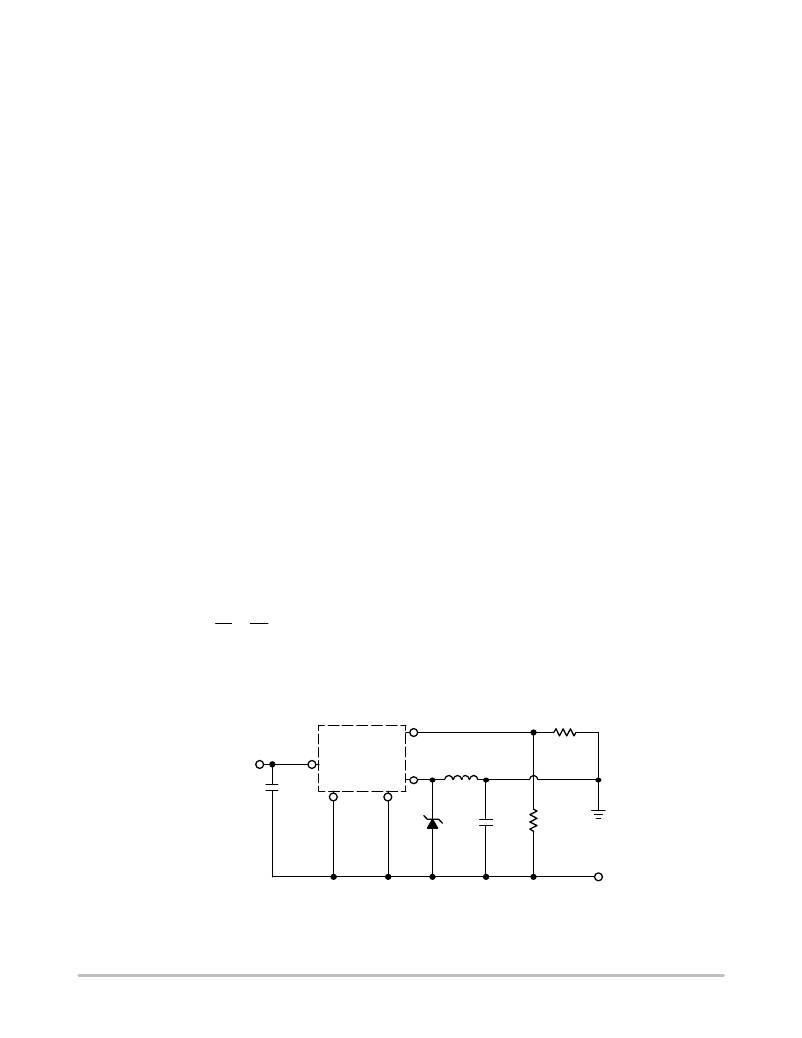
�12� to� 40� V�
�Feedback�
�R4�
�Unregulated�
�DC� Input�
�+V� in�
�LM2596� ?� ADJ�
�L1�
�33� m� H�
�C� in�
�100� m� F/50� V�
�ON/OFF�
�GND�
�D1�
�1N5822�
�C� out�
�220� m� F�
�R3�
�?� 12� V� @� 0.7� A�
�Regulated�
�Output�
�Figure� 22.� Inverting� Buck� ?� Boost� Develops� ?� 12� V�
�http://onsemi.com�
�17�
�相关PDF资料 |
PDF描述 |
|---|---|
| LQG15HN18NJ02D | INDUCTOR 18NH 300MA 0402 |
| LQG15HN15NJ02D | INDUCTOR 15NH 300MA 0402 |
| LM2574DW-ADJR2G | IC REG BUCK ADJ 0.5A 16SOICW |
| LM2574N-3.3G | IC REG BUCK 3.3V 0.5A 8DIP |
| LQG15HN12NJ02D | INDUCTOR 12NH 300MA 0402 |
相关代理商/技术参数 |
参数描述 |
|---|---|
| LM2597HVM-12 | 功能描述:直流/直流开关转换器 RoHS:否 制造商:STMicroelectronics 最大输入电压:4.5 V 开关频率:1.5 MHz 输出电压:4.6 V 输出电流:250 mA 输出端数量:2 最大工作温度:+ 85 C 安装风格:SMD/SMT |
| LM2597HVM-12/NOPB | 功能描述:直流/直流开关转换器 RoHS:否 制造商:STMicroelectronics 最大输入电压:4.5 V 开关频率:1.5 MHz 输出电压:4.6 V 输出电流:250 mA 输出端数量:2 最大工作温度:+ 85 C 安装风格:SMD/SMT |
| LM2597HVM-12/NOPB | 制造商:Texas Instruments 功能描述:DC/DC Converter IC |
| LM2597HVM-3.3 | 功能描述:直流/直流开关转换器 RoHS:否 制造商:STMicroelectronics 最大输入电压:4.5 V 开关频率:1.5 MHz 输出电压:4.6 V 输出电流:250 mA 输出端数量:2 最大工作温度:+ 85 C 安装风格:SMD/SMT |
| LM2597HVM-3.3/NOPB | 功能描述:直流/直流开关转换器 RoHS:否 制造商:STMicroelectronics 最大输入电压:4.5 V 开关频率:1.5 MHz 输出电压:4.6 V 输出电流:250 mA 输出端数量:2 最大工作温度:+ 85 C 安装风格:SMD/SMT |
发布紧急采购,3分钟左右您将得到回复。