- 您现在的位置:买卖IC网 > PDF目录98000 > LM2633MTDX/NOPB (NATIONAL SEMICONDUCTOR CORP) SWITCHING CONTROLLER, 275 kHz SWITCHING FREQ-MAX, PDSO48 PDF资料下载
参数资料
| 型号: | LM2633MTDX/NOPB |
| 厂商: | NATIONAL SEMICONDUCTOR CORP |
| 元件分类: | 稳压器 |
| 英文描述: | SWITCHING CONTROLLER, 275 kHz SWITCHING FREQ-MAX, PDSO48 |
| 封装: | TSSOP-48 |
| 文件页数: | 27/40页 |
| 文件大小: | 1350K |
| 代理商: | LM2633MTDX/NOPB |
第1页第2页第3页第4页第5页第6页第7页第8页第9页第10页第11页第12页第13页第14页第15页第16页第17页第18页第19页第20页第21页第22页第23页第24页第25页第26页当前第27页第28页第29页第30页第31页第32页第33页第34页第35页第36页第37页第38页第39页第40页
Control Loop Design (Continued)
TABLE 5. R1 and R2 Values vs. VID
VID4:0
V
DAC (V)
R
1
R
2
r=
R2/(R1+R2)
00000
2.00
25k
17.1k
0.41
00001
1.95
25k
18.4k
0.42
00010
1.90
25k
17.4k
0.41
00011
1.85
25k
21.4k
0.46
00100
1.80
25k
19.3k
0.43
00101
1.75
25k
22.0k
0.47
00110
1.70
25k
22.1k
0.47
00111
1.65
25k
30.0k
0.55
01000
1.60
25k
24.5k
0.49
01001
1.55
25k
27.3k
0.52
01010
1.50
25k
26.0k
0.51
01011
1.45
25k
34.6k
0.58
01100
1.40
25k
29.3k
0.54
01101
1.35
25k
36.0k
0.59
01110
1.30
25k
36.4k
0.59
01111
NO CPU
25k
64.3k
0.72
10000
1.275
12.5k
23.2k
0.65
10001
1.250
12.5k
25.7k
0.67
10010
1.225
12.5k
24.5k
0.66
10011
1.200
12.5k
32.1k
0.72
10100
1.175
12.5k
27.5k
0.69
10101
1.150
12.5k
33.3k
0.73
10110
1.125
12.5k
33.6k
0.73
10111
1.100
12.5k
56.2k
0.82
11000
1. 075
12.5k
39.6k
0.76
11001
1.050
12.5k
47.4k
0.79
11010
1.025
12.5k
43.4k
0.78
11011
1.000
12.5k
75.0k
0.86
11100
0.975
12.5k
53.7k
0.81
11101
0.95
12.5k
81.8k
0.87
11110
0.925
12.5k
83.7k
0.87
11111
0.900
12.5k
∞
1
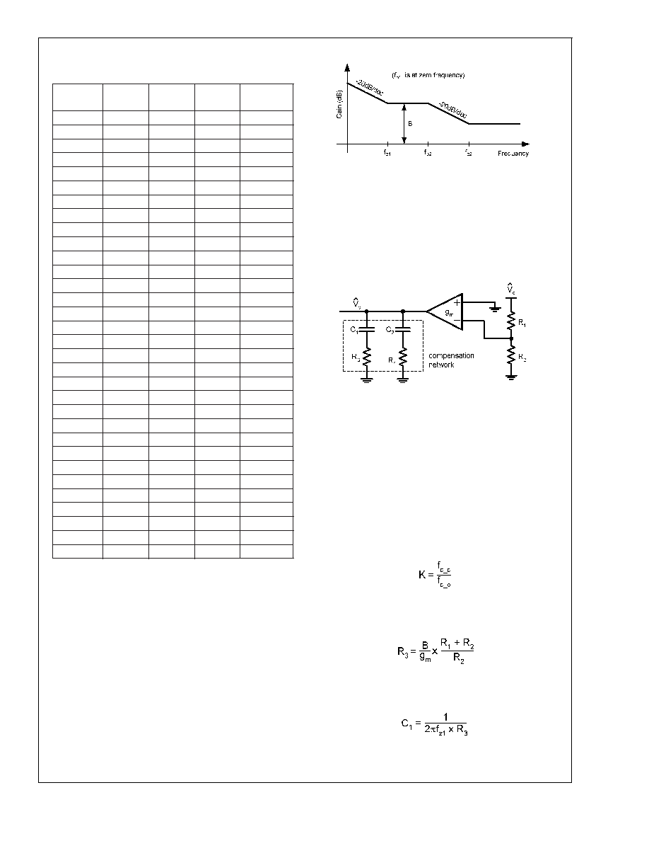
The signal path from output voltage to control voltage is the
feedback path. It typically contains a voltage divider, an error
amplifier and a compensation network. Those are shown In
Figure 7 as R
1,R2, the gm amplifier, and Zc. For Channel 1
of the LM2633, since an R-2R ladder network is used, R
1
and R
2 values change with the VID setting. For information
regarding their values and ratios, refer to
Table 5. For Chan-
nel 2, R
1 and R2 are simply the external voltage divider
resistors.
To achieve the gain shape in
c in Figure 7 should
take the form of two RC branches in parallel, as shown in
Figure 11. In the scheme, C1 and R3 form the first zero f
z1,
C2 and R3 form the second pole f
p2, and C2 and R4 form the
second zero f
z2.
The gain of the compensation network can be calculated as
the following. If the ESR zero frequency f
z is higher than the
low frequency pole f
p, then there should be a 20dB/decade
section from f
p (310 Hz) to fz (8.8 kHz) in the plant gain plot,
such as shown in
Figure 9. Find the frequency where this
section (or the extension of this section) crosses 0dB by
using the following equation:
f
c_o =M fp
(41)
If the desired loop transfer function cross-over frequency is
f
c_c, then the gain of the compensation network at fp should
be:
(42)
To determine the component values in
Figure 11, the follow-
ing equations can be used:
(43)
where B is the desired gain at f
z1, and gm is the transcon-
ductance of the error amplifier.
(44)
20000864
FIGURE 10. 2-Pole 2-Zero (lag-lag) Network Asymptotic
Gain Plot
20000865
FIGURE 11. Compensation Network
LM2633
www.national.com
33
相关PDF资料 |
PDF描述 |
|---|---|
| LM2635MX/NOPB | SWITCHING CONTROLLER, 350 kHz SWITCHING FREQ-MAX, PDSO20 |
| LM26480QSQX-CF/NOPB | 2.4 A SWITCHING REGULATOR, 2500 kHz SWITCHING FREQ-MAX, QCC24 |
| LM26480QSQ-CF/NOPB | 2.4 A SWITCHING REGULATOR, 2500 kHz SWITCHING FREQ-MAX, QCC24 |
| LM26480SQ-BF/NOPB | 2.4 A SWITCHING REGULATOR, 2400 kHz SWITCHING FREQ-MAX, QCC24 |
| LM26480SQX-BF/NOPB | 2.4 A SWITCHING REGULATOR, 2400 kHz SWITCHING FREQ-MAX, QCC24 |
相关代理商/技术参数 |
参数描述 |
|---|---|
| LM2635 | 制造商:NSC 制造商全称:National Semiconductor 功能描述:5-Bit Programmable Synchronous Buck Regulator Controller |
| LM2635A WAF | 制造商:Texas Instruments 功能描述: |
| LM2635M | 制造商:Rochester Electronics LLC 功能描述: 制造商:Texas Instruments 功能描述: |
| LM2635M/NOPB | 功能描述:IC REG SYNCH BUCK 5-BIT 20-SOIC RoHS:是 类别:集成电路 (IC) >> PMIC - 电源管理 - 专用 系列:- 应用说明:Ultrasound Imaging Systems Application Note 产品培训模块:Lead (SnPb) Finish for COTS Obsolescence Mitigation Program 标准包装:37 系列:- 应用:医疗用超声波成像,声纳 电流 - 电源:- 电源电压:2.37 V ~ 6 V 工作温度:0°C ~ 70°C 安装类型:表面贴装 封装/外壳:56-WFQFN 裸露焊盘 供应商设备封装:56-TQFN-EP(8x8) 包装:管件 |
| LM2635MX | 功能描述:IC REG SYNCH BUCK 5-BIT 20-SOIC RoHS:是 类别:集成电路 (IC) >> PMIC - 电源管理 - 专用 系列:- 应用说明:Ultrasound Imaging Systems Application Note 产品培训模块:Lead (SnPb) Finish for COTS Obsolescence Mitigation Program 标准包装:37 系列:- 应用:医疗用超声波成像,声纳 电流 - 电源:- 电源电压:2.37 V ~ 6 V 工作温度:0°C ~ 70°C 安装类型:表面贴装 封装/外壳:56-WFQFN 裸露焊盘 供应商设备封装:56-TQFN-EP(8x8) 包装:管件 |
发布紧急采购,3分钟左右您将得到回复。