- 您现在的位置:买卖IC网 > PDF目录98000 > LM2633MTDX/NOPB (NATIONAL SEMICONDUCTOR CORP) SWITCHING CONTROLLER, 275 kHz SWITCHING FREQ-MAX, PDSO48 PDF资料下载
参数资料
| 型号: | LM2633MTDX/NOPB |
| 厂商: | NATIONAL SEMICONDUCTOR CORP |
| 元件分类: | 稳压器 |
| 英文描述: | SWITCHING CONTROLLER, 275 kHz SWITCHING FREQ-MAX, PDSO48 |
| 封装: | TSSOP-48 |
| 文件页数: | 6/40页 |
| 文件大小: | 1350K |
| 代理商: | LM2633MTDX/NOPB |
第1页第2页第3页第4页第5页当前第6页第7页第8页第9页第10页第11页第12页第13页第14页第15页第16页第17页第18页第19页第20页第21页第22页第23页第24页第25页第26页第27页第28页第29页第30页第31页第32页第33页第34页第35页第36页第37页第38页第39页第40页
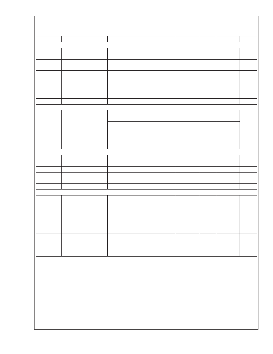
Electrical Characteristics (Continued)
V
CC = +15V unless otherwise indicated under the Conditions column. Typicals and limits appearing in plain type apply for TA
=T
J = +25C. Limits appearing in boldface type apply over 40C to +125C.
Symbol
Parameter
Conditions
Min
Typ
Max
Units
Error Amplifier
I
fb2
Feedback Input Bias
Current, Channel 2
V
FB2 = 1.36V
18
nA
I
fb3
Feedback Input Bias
Current, Channel 3
V
FB3 = 1.36V
70
nA
I
comp1,
I
comp2
COMP Output Sink
Current
V
FB1 = 150% of measured 1.4V DAC,
V
FB2 = 150% of measured bandgap,
V
COMP1 =VCOMP2 =1V
91
A
V
comp_max
COMP Pin Maximum
Voltage
tbd
1.96
V
Gm
Transconductance
576
mho
DAC Output and V
FB2
V
dac
Channel 1 DAC Output
Voltage Accuracy
VCOMP1 = 1V, DAC codes from 1.3V
to 1.6V
2.0
%
VCOMP1 = 1V, DAC codes from
0.925V to 1.25V and from 1.65V to
2.00V
2.2
V
fb2
Channel 2 DC Output
Voltage Accuracy
COMP2 pin from 0.5V to 1.8V
1.212
1.238
1.264
V
Linear Regulator Controller
V
fb3
Channel 3 DC Output
Voltage Accuracy
1.209
1.24
1.271
V
g3_sk
G3 Sink Current
20
A
I
g3_sc
G3 Minimum Source
Current
20
mA
V
g3_max
G3 Maximum Voltage
3.6
V
Logic Inputs and Outputs
V
ih
Minimum High Level
Input Voltage (FPWM,
VID0-VID4)
2.2
V
il
Maximum Low Level
Input Voltage (FPWM,
ON/SS1, ON/SS2,
VID0-VID4)
0.7
V
I
oh_pg
PGOOD Output High
Current
PGOOD = 5.7V (Note 23)
5A
V
ol_pg
PGOOD Output Low
Voltage
PGOOD Sinking 20 A
0.3
V
Note 11: Absolute maximum ratings indicate limits beyond which damage to the device may occur. Operating Ratings are conditions under which operation of the
device is guaranteed. For guaranteed performance limits and associated test conditions, see the Electrical Characteristics table.
Note 12: Maximum allowable power dissipation is calculated by using PDMAX =(TJMAX -TA)/θJA, where TJMAX is the maximum junction temperature, TA is the
ambient temperature and
θJA is the junction-to-ambient thermal resistance of the specified package. The 1.56W rating results from using 150C, 25C, and 80C/W
for TJMAX,TA, and θJA respectively. A θJA of 90C/W represents the worst-case condition of no heat sinking of the 48-pin TSSOP. Heat sinking allows the safe
dissipation of more power. The Absolute Maximum power dissipation should be derated by 12.5mW per C above 25C ambient. The LM2633 actively limits its
junction temperature to about 150C.
Note 13: For detailed information on soldering plastic small-outline packages, refer to the Packaging Databook available from National Semiconductor Corporation.
Note 14: Except for ILIM1 and ILIM2 pins, which are 1.5kV. For testing purposes, ESD was applied using the human-body model, a 100pF capacitor discharged
through a 1.5k
resistor.
Note 15: A typical is the center of characterization data taken with TA =TJ = 25C. Typical data are not guaranteed.
Note 16: All limits are guaranteed. All electrical characteristics having room-temperature limits are tested during production with TA =TJ = 25C. All hot and cold
limits are guaranteed by correlating the electrical characteristics to process and temperature variations and applying statistical process control.
Note 17: This test simulates heavy load condition by changing COMP pin voltage.
Note 18: This parameter indicates how much current the LM2633 is drawing from the input supply when it is functioning but not driving external MOSFETs or a
bipoloar transistor.
LM2633
www.national.com
14
相关PDF资料 |
PDF描述 |
|---|---|
| LM2635MX/NOPB | SWITCHING CONTROLLER, 350 kHz SWITCHING FREQ-MAX, PDSO20 |
| LM26480QSQX-CF/NOPB | 2.4 A SWITCHING REGULATOR, 2500 kHz SWITCHING FREQ-MAX, QCC24 |
| LM26480QSQ-CF/NOPB | 2.4 A SWITCHING REGULATOR, 2500 kHz SWITCHING FREQ-MAX, QCC24 |
| LM26480SQ-BF/NOPB | 2.4 A SWITCHING REGULATOR, 2400 kHz SWITCHING FREQ-MAX, QCC24 |
| LM26480SQX-BF/NOPB | 2.4 A SWITCHING REGULATOR, 2400 kHz SWITCHING FREQ-MAX, QCC24 |
相关代理商/技术参数 |
参数描述 |
|---|---|
| LM2635 | 制造商:NSC 制造商全称:National Semiconductor 功能描述:5-Bit Programmable Synchronous Buck Regulator Controller |
| LM2635A WAF | 制造商:Texas Instruments 功能描述: |
| LM2635M | 制造商:Rochester Electronics LLC 功能描述: 制造商:Texas Instruments 功能描述: |
| LM2635M/NOPB | 功能描述:IC REG SYNCH BUCK 5-BIT 20-SOIC RoHS:是 类别:集成电路 (IC) >> PMIC - 电源管理 - 专用 系列:- 应用说明:Ultrasound Imaging Systems Application Note 产品培训模块:Lead (SnPb) Finish for COTS Obsolescence Mitigation Program 标准包装:37 系列:- 应用:医疗用超声波成像,声纳 电流 - 电源:- 电源电压:2.37 V ~ 6 V 工作温度:0°C ~ 70°C 安装类型:表面贴装 封装/外壳:56-WFQFN 裸露焊盘 供应商设备封装:56-TQFN-EP(8x8) 包装:管件 |
| LM2635MX | 功能描述:IC REG SYNCH BUCK 5-BIT 20-SOIC RoHS:是 类别:集成电路 (IC) >> PMIC - 电源管理 - 专用 系列:- 应用说明:Ultrasound Imaging Systems Application Note 产品培训模块:Lead (SnPb) Finish for COTS Obsolescence Mitigation Program 标准包装:37 系列:- 应用:医疗用超声波成像,声纳 电流 - 电源:- 电源电压:2.37 V ~ 6 V 工作温度:0°C ~ 70°C 安装类型:表面贴装 封装/外壳:56-WFQFN 裸露焊盘 供应商设备封装:56-TQFN-EP(8x8) 包装:管件 |
发布紧急采购,3分钟左右您将得到回复。