- 您现在的位置:买卖IC网 > PDF目录44549 > LM2636MTCX/NOPB (NATIONAL SEMICONDUCTOR CORP) SWITCHING CONTROLLER, 2000 kHz SWITCHING FREQ-MAX, PDSO20 PDF资料下载
参数资料
| 型号: | LM2636MTCX/NOPB |
| 厂商: | NATIONAL SEMICONDUCTOR CORP |
| 元件分类: | 稳压器 |
| 英文描述: | SWITCHING CONTROLLER, 2000 kHz SWITCHING FREQ-MAX, PDSO20 |
| 封装: | PLASTIC, TSSOP-20 |
| 文件页数: | 16/17页 |
| 文件大小: | 372K |
| 代理商: | LM2636MTCX/NOPB |
Applications Information (Continued)
the
error
amplifier
is
then
compared
with
an
internally generated PWM ramp signal and the result of the
comparison is a series of pulses with certain duty ratios.
These pulses are used to control the turn-on and turn-off of
the MOSFET gate drivers. In this way, the error in the output
voltage gets “compensated” or cancelled by the change in
the duty ratio of the FET switches. During a large load tran-
sient, depending on the compensation design, the change in
duty ratio can be as fast as less than one switching cycle.
Refer to Design Considerations section for more details.
Besides the usual voltage mode feedback control loop, the
LM2636 also has a pair of fast comparators (the MIN and
MAX comparators) to help maintain the output voltage dur-
ing a large and fast load transient. The trip points of the com-
parators are set to ±5% of the DAC output voltage. When
the load transient is so large that the output voltage goes
outside the ±5% window, the MIN or MAX comparator will
bypass the primary voltage control loop and immediately set
the duty ratio to either maximum value or to zero. This pro-
vides the fastest possible way to react to such a large load
transient in a classical buck converter.
Power Good Signal
The power good signal is used to indicate that the output
voltage is within specified range. In the LM2636, the range is
set to a ±10% window of the DAC output voltage. During soft
start, the power good signal is always low. At the end of the
soft start session,the output voltage is checked and the
PWRGD pin will be asserted if the voltage is within specified
range.
Over Voltage Protection
When the output voltage exceeds 115% of the DAC output
voltage after the end of soft start, the LM2636 will enter over
voltage protection mode in which it shuts itself down. The up-
per gate driver is held low while the lower gate driver is held
high. PWRGD will be low. For LM2636 to recover from OVP
mode, either OUTEN or V
CC voltage has to be toggled. An-
other more subtle way to recover is to float all the VID pins
and reapply the correct code.
Current Limit
Current limit is realized by sensing the V
DS voltage of the
high side MOSFET when it is on. Since the r
DS_ON of a
MOSFET is a known value, current through the MOSFET
can be known by monitoring V
DS. The relationship between
the three parameters is:
To implement the current limit function, an external resistor
R
IMAX is need. The resistor should be connected between
the drain of the high side MOSFET and the IMAX pin. A con-
stant current of around 180 A is forced into the IMAX pin
and causes a fixed voltage drop across the R
IMAX resistor.
This voltage drop is then compared with the V
DS of the high
side MOSFET and if the latter is higher, over current is
reached. So the appropriate value of R
IMAX
for a pre-
determined current limit level I
LIM can be calculated by the
following equation:
For example, if we know that the r
DS_ON of the MOSFET is
20 m
, and the current limit we want to set is 20A, then we
should choose the value of R
IMAX to be 2.2 k.
To provide the greatest protection over the high side MOS-
FET, cycle by cycle protection is implemented. The sampling
of the V
DS starts as early as about 300 ns after the switch is
turned on. Whenever an over current condition is detected,
the high side switch is immediately turned off and the low
side switch turned on, until the next switching cycle comes.
The delay of 300 ns is to circumvent switching noise when
the MOSFET is first turned on.
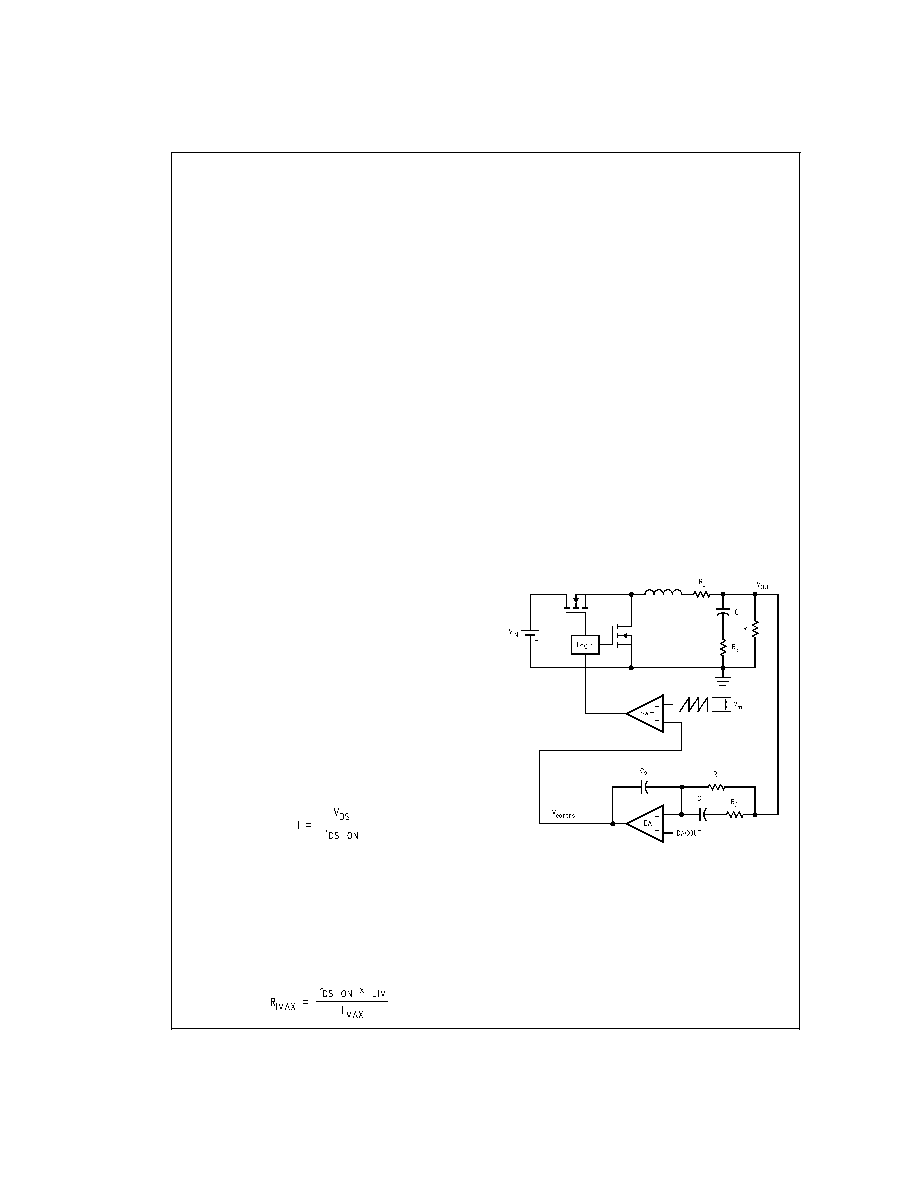
DESIGN CONSIDERATIONS
Control Loop Compensation
A switching regulator should be properly compensated to
achieve a stable condition. For a synchronous buck regula-
tor that needs to meet stringent load transient requirement
such as a Pentium II MPU core voltage supply, a simple
2-pole-1-zero compensation network should suffice, such as
the one shown in
Figure 4 (C
1,C2,R1 and R2). This is be-
cause the ESR zero of the typical output capacitors is low
enough to make the control-to-output transfer function a
single-pole-roll-off.
As an example, let us figure out the values of the compensa-
tion network components in
Figure 4. Assume the following
parameters:R=20
,R
L =20m,RC =9m,L =2H,
C = 7.5 mF, V
IN =5V, Vm = 2V and switching frequency
= 300 kHz. These parameters are based on the typical appli-
cation in
Figure 1. Notice R
L is the sum of the inductor DC re-
sistance and the on resistance of the MOSFETs.
DS100834-9
FIGURE 4. Buck Converter from a Control Point of
View
LM2636
www.national.com
8
相关PDF资料 |
PDF描述 |
|---|---|
| LM2637M/NOPB | SWITCHING CONTROLLER, 1000 kHz SWITCHING FREQ-MAX, PDSO24 |
| LM2637MWC | SWITCHING CONTROLLER, 1000 kHz SWITCHING FREQ-MAX, UUC |
| LM2639MX/NOPB | SWITCHING CONTROLLER, 8700 kHz SWITCHING FREQ-MAX, PDSO24 |
| LM2639M/NOPB | SWITCHING CONTROLLER, 8700 kHz SWITCHING FREQ-MAX, PDSO24 |
| LM2639MWC | SWITCHING CONTROLLER, 8700 kHz SWITCHING FREQ-MAX, UUC |
相关代理商/技术参数 |
参数描述 |
|---|---|
| LM2636MX | 制造商:Texas Instruments 功能描述: |
| LM2636MX/NOPB | 功能描述:IC CTRLR PROG REG 5BIT 20-SOIC RoHS:是 类别:集成电路 (IC) >> PMIC - 电源管理 - 专用 系列:- 应用说明:Ultrasound Imaging Systems Application Note 产品培训模块:Lead (SnPb) Finish for COTS Obsolescence Mitigation Program 标准包装:37 系列:- 应用:医疗用超声波成像,声纳 电流 - 电源:- 电源电压:2.37 V ~ 6 V 工作温度:0°C ~ 70°C 安装类型:表面贴装 封装/外壳:56-WFQFN 裸露焊盘 供应商设备封装:56-TQFN-EP(8x8) 包装:管件 |
| LM2637 | 制造商:未知厂家 制造商全称:未知厂家 功能描述: |
| LM2637A E WAF | 制造商:Texas Instruments 功能描述: |
| LM2637M | 制造商:OC White Company 功能描述:LDO Cntrlr REG CTRLR 1.3V to 3.5V 24-Pin SOIC W Rail |
发布紧急采购,3分钟左右您将得到回复。