- 您现在的位置:买卖IC网 > PDF目录30754 > LM4879IBPX/NOPB (NATIONAL SEMICONDUCTOR CORP) 1.1 W, 1 CHANNEL, AUDIO AMPLIFIER, PBGA8 PDF资料下载
参数资料
| 型号: | LM4879IBPX/NOPB |
| 厂商: | NATIONAL SEMICONDUCTOR CORP |
| 元件分类: | 音频/视频放大 |
| 英文描述: | 1.1 W, 1 CHANNEL, AUDIO AMPLIFIER, PBGA8 |
| 封装: | MO-211BC, MICRO, SMD-8 |
| 文件页数: | 5/25页 |
| 文件大小: | 793K |
| 代理商: | LM4879IBPX/NOPB |
Application Information (Continued)
Selection Of Input Capacitor Size
Large input capacitors are both expensive and space hungry
for portable designs. Clearly, a certain sized capacitor is
needed to couple in low frequencies without severe attenu-
ation. But in many cases the speakers used in portable
systems, whether internal or external, have little ability to
reproduce signals below 100 Hz to 150 Hz. Thus, using a
large input capacitor may not increase actual system perfor-
mance.
In addition to system cost and size, click and pop perfor-
mance is effected by the size of the input coupling capacitor,
C
i. A larger input coupling capacitor requires more charge to
reach its quiescent DC voltage (nominally 1/2 V
DD). This
charge comes from the output via the feedback and is apt to
create pops upon device enable. Thus, by minimizing the
capacitor size based on necessary low frequency response,
turn-on pops can be minimized.
Besides minimizing the input capacitor size, careful consid-
eration should be paid to the bypass capacitor value. Bypass
capacitor, C
B, is the most critical component to minimize
turn-on pops since it determines how fast the LM4879 turns
on. The slower the LM4879’s outputs ramp to their quiescent
DC voltage (nominally 1/2 V
DD), the smaller the turn-on pop.
Choosing C
B equal to 1.0 F along with a small value of Ci
(in the range of 0.1 F to 0.39 F), should produce a virtually
clickless and popless shutdown function. While the device
will function properly, (no oscillations or motorboating), with
C
B equal to 0.1 F, the device will be much more susceptible
to turn-on clicks and pops. Thus, a value of C
B equal to
1.0 F is recommended in all but the most cost sensitive
designs.
AUDIO POWER AMPLIFIER DESIGN
A 1W/8
Audio Amplifier
Given:
Power Output
1 Wrms
Load Impedance
8
Input Level
1 Vrms
Input Impedance
20 k
Bandwidth
100 Hz–20 kHz ± 0.25 dB
A designer must first determine the minimum supply rail to
obtain the specified output power. By extrapolating from the
Output Power vs Supply Voltage graphs in the Typical Per-
formance Characteristics section, the supply rail can be
easily found. A second way to determine the minimum sup-
ply rail is to calculate the required V
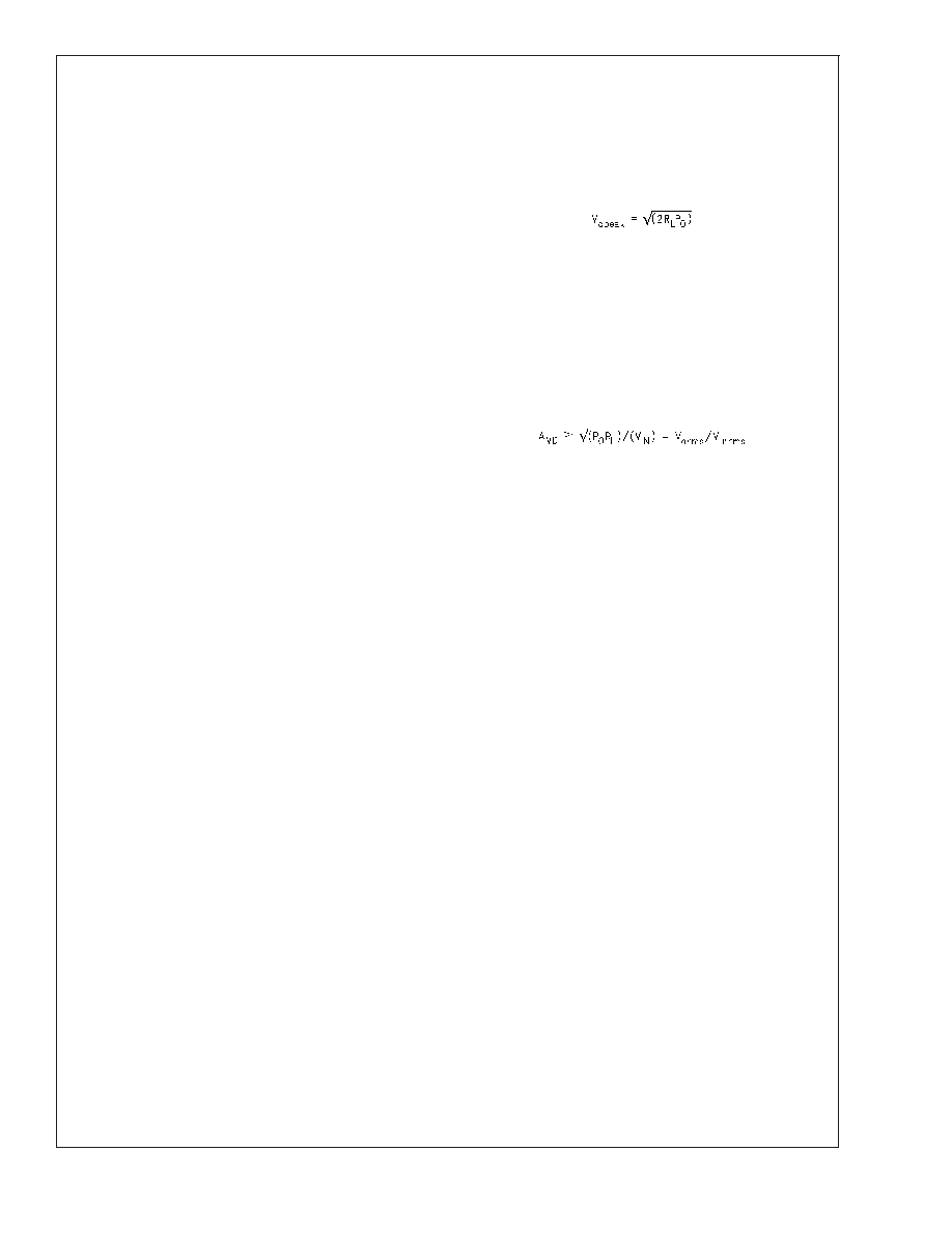
opeak using Equation 2
and add the output voltage. Using this method, the minimum
supply voltage would be (V
opeak +(VODTOP +VODBOT)), where
V
ODBOT and VODTOP are extrapolated from the Dropout Volt-
age vs Supply Voltage curve in the Typical Performance
Characteristics section.
(2)
5V is a standard voltage, in most applications, chosen for the
supply rail. Extra supply voltage creates headroom that al-
lows the LM4879 to reproduce peaks in excess of 1W with-
out producing audible distortion. At this time, the designer
must make sure that the power supply choice along with the
output impedance does not violate the conditions explained
in the Power Dissipation section.
Once the power dissipation equations have been addressed,
the required differential gain can be determined from Equa-
tion 3.
(3)
A
VD =(Rf/Ri)2
From Equation 3, the minimum A
VD is 2.83; use AVD =3.
Since the desired input impedance was 20 k
, and with a
A
VD of 3, a ratio of 1.5:1 of Rf to Ri results in an allocation of
R
i =20k
and R
f =30k
. The final design step is to
address the bandwidth requirements which must be stated
as a pair of 3 dB frequency points. Five times away from a
3 dB point is 0.17 dB down from passband response which
is better than the required ±0.25 dB specified.
f
L = 100 Hz/5 = 20 Hz
f
H =20kHz*5=100 kHz
As stated in the External Components section, R
i in con-
junction with C
i create a highpass filter.
C
i
≥ 1/(2π*20 k*20 Hz) = 0.397 F; use 0.39 F
The high frequency pole is determined by the product of the
desired frequency pole, f
H, and the differential gain, AVD.
With a A
VD = 3 and fH = 100 kHz, the resulting GBWP =
300 kHz which is much smaller than the LM4879 GBWP of
10 MHz. This figure displays that if a designer has a need to
design an amplifier with a higher differential gain, the
LM4879 can still be used without running into bandwidth
limitations.
LM4879
www.national.com
13
相关PDF资料 |
PDF描述 |
|---|---|
| LM4879IBP/NOPB | 1.1 W, 1 CHANNEL, AUDIO AMPLIFIER, PBGA8 |
| LM4879ITLX/NOPB | 1.1 W, 1 CHANNEL, AUDIO AMPLIFIER, PBGA9 |
| LM4880-D08-T | 0.35 W, 2 CHANNEL, AUDIO AMPLIFIER, PDIP8 |
| LM4880-SH2-R | 0.35 W, 2 CHANNEL, AUDIO AMPLIFIER, PDSO8 |
| LM4880-SH2-T | 0.35 W, 2 CHANNEL, AUDIO AMPLIFIER, PDSO8 |
相关代理商/技术参数 |
参数描述 |
|---|---|
| LM4879ITL | 制造商:Texas Instruments 功能描述:AMP AUDIO BOOMER 1.1W SMD BUMP-9 |
| LM4879ITL/NOPB | 功能描述:音频放大器 RoHS:否 制造商:STMicroelectronics 产品:General Purpose Audio Amplifiers 输出类型:Digital 输出功率: THD + 噪声: 工作电源电压:3.3 V 电源电流: 最大功率耗散: 最大工作温度: 安装风格:SMD/SMT 封装 / 箱体:TQFP-64 封装:Reel |
| LM4879ITLX | 制造商:NSC 制造商全称:National Semiconductor 功能描述:1.1 Watt Audio Power Amplifier |
| LM4879ITLX/NOPB | 功能描述:音频放大器 RoHS:否 制造商:STMicroelectronics 产品:General Purpose Audio Amplifiers 输出类型:Digital 输出功率: THD + 噪声: 工作电源电压:3.3 V 电源电流: 最大功率耗散: 最大工作温度: 安装风格:SMD/SMT 封装 / 箱体:TQFP-64 封装:Reel |
| LM4879ITP | 功能描述:IC AMP AUDIO PWR 1.1W MONO 8USMD RoHS:是 类别:集成电路 (IC) >> 线性 - 音頻放大器 系列:Boomer® 产品培训模块:Lead (SnPb) Finish for COTS Obsolescence Mitigation Program 标准包装:2,500 系列:DirectDrive® 类型:D 类 输出类型:1-通道(单声道),带立体声耳机 在某负载时最大输出功率 x 通道数量:930mW x 1 @ 8 欧姆; 40mW x 2 @ 16 欧姆 电源电压:2.7 V ~ 5.5 V 特点:消除爆音,差分输入,I²C,静音,关闭,音量控制 安装类型:表面贴装 供应商设备封装:25-WLP(2.09x2.09) 封装/外壳:25-WFBGA,WLCSP 包装:带卷 (TR) 其它名称:MAX97000EWA+T-ND |
发布紧急采购,3分钟左右您将得到回复。