- 您现在的位置:买卖IC网 > PDF目录20330 > LM5051MA/NOPB (National Semiconductor)IC ORING FET CTRLR 8SOIC PDF资料下载
参数资料
| 型号: | LM5051MA/NOPB |
| 厂商: | National Semiconductor |
| 文件页数: | 4/23页 |
| 文件大小: | 0K |
| 描述: | IC ORING FET CTRLR 8SOIC |
| 标准包装: | 95 |
| 应用: | 冗余电源 |
| FET 型: | N 沟道 |
| 输出数: | 1 |
| 内部开关: | 无 |
| 电源电压: | 36 V ~ 100 V |
| 电流 - 电源: | 400µA |
| 工作温度: | -40°C ~ 125°C |
| 安装类型: | 表面贴装 |
| 封装/外壳: | 8-SOIC(0.154",3.90mm 宽) |
| 供应商设备封装: | 8-SOICN |
| 包装: | 管件 |
�� ���
���
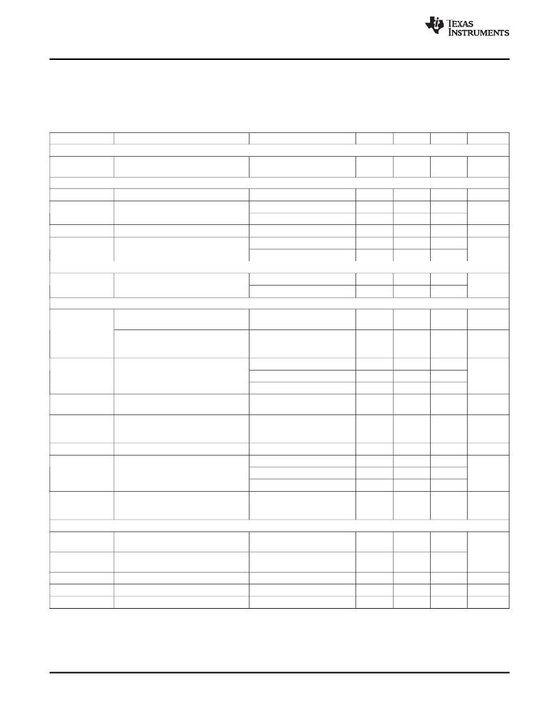
���SNVS702D� –� OCTOBER� 2011� –� REVISED� MARCH� 2013�
��Electrical� Characteristics�
�Limits� in� standard� type� are� for� T� J� =� 25°C� only;� limits� in� boldface� type� apply� over� the� operating� junction� temperature� (T� J� )�
�range� of� -40°C� to� +125°C.� Minimum� and� Maximum� limits� are� ensured� through� test,� design,� or� statistical� correlation.� Typical�
�values� represent� the� most� likely� parametric� norm� at� T� J� =� 25°C,� and� are� provided� for� reference� purposes� only.� Unless�
�otherwise� stated� all� conditions� and� measurements� are� referenced� to� device� pin� 7� (INP/VSS),� and� the� following� conditions�
�apply:� V� LINE� =� 48.0V,� V� INN� =� -150� mV,� V� OFF� =� 0.0V,� C� GATE� = 47 nF, C� VCC� = 0.1 μF, and T� J� =� 25°C.�
�Symbol�
�Parameter�
�Conditions�
�Min�
�Typ�
�Max�
�Unit�
�LINE� Pin�
�I� LINE�
�LINE� Pin� current�
�V� LINE� =� 48.0V�
�VCC� Pin� =� Open�
�-�
�690�
�780�
�μ� A�
�VCC� Pin�
�VCC�
�V� Z�
�Δ� V� Z�
�I� VCC�
�Operating� Voltage� Range�
�VCC� Shunt� Zener� Voltage�
�Shunt� Zener� Regulation�
�Supply� Current�
�LINE� Pin� =� Open�
�I� VCC� =� 2� mA�
�I� VCC� =� 10� mA�
�I� VCC� =� 2� mA� to� 10� mA�
�V� VCC� =� V� Z� -� 100mV�
�V� VCC� =� 5.0V�
�4.50�
�11.9�
�12.5�
�-�
�-�
�-�
�-�
�13.0�
�13.5�
�0.50�
�1.0�
�0.4�
�V� Z�
�14.3�
�14.5�
�1.11�
�1.50�
�1.10�
�V�
�V�
�V�
�mA�
�INN� Pin�
�I� INN�
�INN� Pin� Current�
�V� INN� =� 0.0V�
�V� INN� =� 90V�
�-�
�-�
�3.1�
�0.04�
�-�
�-�
�μ� A�
�GATE�
�GATE� Charge� Current�
�V� GATE� =� 5.5V�
�V� INN� =� -150mV�
�0.28�
�0.66�
�0.95�
�mA�
�I� GATE�
�V� GATE� =� 5.5V�
�GATE� Discharge� Current�
�V� INN� =� -150� mV� to� +300� mV�
�2.4�
�3.5�
�-�
�A�
�t� ≤� 10� ms�
�V� LINE� =� 48.0V�
�-�
�13.0�
�-�
�V� GATE�
�GATE� Pin� High� Voltage�
�V� VCC� =� 10.25V,� LINE� =� Open�
�9.98�
�10.2�
�-�
�V�
�V� VCC� =� 5.0V,� LINE=� Open�
�4.70�
�4.95�
�-�
�V� SD(REV)�
�Reverse� Threshold�
�V� INN� going� negative� until� Gate�
�Drive� Turns� ON�
�-112.2�
�-45�
�+11.4�
�mV�
�Δ� V� SD(REV)�
�Reverse� Threshold� Hysteresis�
�V� INN� going� positive� from�
�V� SD(REV)� Threshold� until� Gate�
�-�
�50�
�-�
�mV�
�Drive� Turns� OFF�
�V� SD(REG)�
�Regulated� V� INP/VSS� to� V� INN� Threshold�
�-10.8�
�12�
�30.8�
�mV�
�C� GATE� =� 0�
�t� GATE(REV)�
�t� GATE(OFF)�
�Gate� Capacitance� Discharge� Time� at�
�Forward� to� Reverse� Transition�
��Gate� Capacitance� Discharge� Time� at�
�OFF� pin� Low� to� High� Transition�
�(1)�
�C� GATE� =� 10� nF�
�C� GATE� =� 47� nF�
�C� GATE� =� 47� nF�
�(1)�
�(1)�
�(2)�
�-�
�-�
�-�
�-�
�34�
�60�
�90�
�120�
�50�
�-�
�230�
�-�
�ns�
�ns�
��OFF� Pin�
�V� OFF(IH)�
�V� OFF(IL)�
�Δ� V� OFF�
�I� OFF(IH)�
�I� OFF(IL)�
�OFF� Input� High� Threshold� Voltage�
�OFF� Input� Low� Threshold� Voltage�
�OFF� Threshold� Voltage� Hysteresis�
�OFF� Pin� Internal� Pull-down�
�V� INN� =� -400� mV�
�V� OFF� Rising� until� Gate� is� Low�
�V� INN� =� -400� mV�
�V� OFF� Falling� until� Gate� is� High�
�V� OFF(IH)� -� V� OFF(IL)�
�V� OFF� =� 5.0V�
�V� OFF� =� 0.0V�
�1.28�
�-�
�-�
�-�
�-�
�1.50�
�1.48�
�20�
�4.6�
�-0.03�
�1.65�
�-�
�-�
�6.00�
�-�
�V�
�mV�
�μA�
�μA�
�(1)�
�(2)�
�Time� from� V� INN� voltage� transition� from� -200� mV� to� +500� mV� until� Gate� pin� voltage� falls� to� ≤� 1.00V.� See� Figure� 6�
�Time� from� V� OFF� voltage� transition� from� 0.0V� to� 5.0V� until� GATE� pin� voltage� falls� to� ≤� 1.0V.� See� Figure� 7�
�4�
��Product� Folder� Links:� LM5051�
�Copyright� ?� 2011–2013,� Texas� Instruments� Incorporated�
�相关PDF资料 |
PDF描述 |
|---|---|
| A101J15C0GL5UAA | CAP CER 100PF 500V 5% NP0 AXIAL |
| LM5051MAE/NOPB | IC ORING FET CTRLR 8SOIC |
| A101J15C0GL5TAA | CAP CER 100PF 500V 5% NP0 AXIAL |
| T95R397K6R3CZAS | CAP TANT 390UF 6.3V 10% 2824 |
| B140HB-13 | DIODE SCHOTTKY 40V 1A SMB |
相关代理商/技术参数 |
参数描述 |
|---|---|
| LM5051MAX/NOPB | 功能描述:热插拔功率分布 Lo Side OR-ing FET Cntlr RoHS:否 制造商:Texas Instruments 产品:Controllers & Switches 电流限制: 电源电压-最大:7 V 电源电压-最小:- 0.3 V 工作温度范围: 功率耗散: 安装风格:SMD/SMT 封装 / 箱体:MSOP-8 封装:Tube |
| LM5056 | 制造商:TI 制造商全称:Texas Instruments 功能描述:High-Voltage System Power Management Device with PMBusa?¢ |
| LM5056A | 制造商:TI 制造商全称:Texas Instruments 功能描述:High-Voltage System Power Management Device with PMBusa?¢ |
| LM5056APMH/NOPB | 功能描述:PMIC 解决方案 Hi Vtg System Pwr Mgmt IC RoHS:否 制造商:Texas Instruments 安装风格:SMD/SMT 封装 / 箱体:QFN-24 封装:Reel |
| LM5056APMHE/NOPB | 功能描述:PMIC 解决方案 Hi Vtg System Pwr Mgmt IC RoHS:否 制造商:Texas Instruments 安装风格:SMD/SMT 封装 / 箱体:QFN-24 封装:Reel |
发布紧急采购,3分钟左右您将得到回复。