- 您现在的位置:买卖IC网 > PDF目录30759 > LMH6715MAXEP (NATIONAL SEMICONDUCTOR CORP) 1 CHANNEL, VIDEO AMPLIFIER, PDSO8 PDF资料下载
参数资料
| 型号: | LMH6715MAXEP |
| 厂商: | NATIONAL SEMICONDUCTOR CORP |
| 元件分类: | 音频/视频放大 |
| 英文描述: | 1 CHANNEL, VIDEO AMPLIFIER, PDSO8 |
| 封装: | PLASTIC, SOIC-8 |
| 文件页数: | 3/13页 |
| 文件大小: | 489K |
| 代理商: | LMH6715MAXEP |
Application Introduction (Continued)
Careful attention to parasitic capacitances is critical to
achieving
the
best
settling
time
performance.
The
LMH6715EP has a typical short term settling time to 0.05%
of 12ns for a 2V step. Also, the amplifier is virtually free of
any long term thermal tail effects at low gains.
When measuring settling time, a solid ground plane should
be used in order to reduce ground inductance which can
cause common-ground-impedance coupling. Power supply
and ground trace parasitic capacitances and the load ca-
pacitance will also affect settling time.
Placing a series resistor (R
s) at the output pin is recom-
mended for optimal settling time performance when driving a
capacitive load. The Typical Performance plot labeled “R
S
and Settling Time vs. Capacitive Load” provides a means for
selecting a value of R
s for a given capacitive load.
DC & NOISE PERFORMANCE
A current-feedback amplifier’s input stage does not have
equal nor correlated bias currents, therefore they cannot be
canceled and each contributes to the total DC offset voltage
at the output by the following equation:
The input resistance is the resistance looking from the non-
inverting input back toward the source. For inverting DC-
offset calculations, the source resistance seen by the input
resistor R
g must be included in the output offset calculation
as a part of the non-inverting gain equation. Application note
OA-7 gives several circuits for DC offset correction. The
noise currents for the inverting and non-inverting inputs are
graphed in the Typical Performance plot labeled “Equivalent
Input Noise”. A more complete discussion of amplifier input-
referred noise and external resistor noise contribution can be
found in OA-12.
DIFFERENTIAL GAIN & PHASE
The LMH6715EP can drive multiple video loads with very
low differential gain and phase errors. The Typical Perfor-
mance plots labeled “Differential Gain vs. Frequency” and
“Differential Phase vs. Frequency” show performance for
loads from 1 to 4. The Electrical Characteristics table also
specifies performance for one 150
load at 4.43MHz. For
NTSC video, the performance specifications also apply. Ap-
plication note OA-24 “Measuring and Improving Differential
Gain & Differential Phase for Video”, describes in detail the
techniques used to measure differential gain and phase.
I/O VOLTAGE & OUTPUT CURRENT
The usable common-mode input voltage range (CMIR) of
the LMH6715EP specified in the Electrical Characteristics
table of the data sheet shows a range of ±2.2 volts. Exceed-
ing this range will cause the input stage to saturate and clip
the output signal.
The output voltage range is determined by the load resistor
and the choice of power supplies. With ±5 volts the class A/B
output driver will typically drive ±3.9V into a load resistance
of 100
. Increasing the supply voltages will change the
common-mode input and output voltage swings while at the
same time increase the internal junction temperature.
Applications Circuits
SINGLE-TO-DIFFERENTIAL LINE DRIVER
The LMH6715EP’s well matched AC channel-response al-
lows a single-ended input to be transformed to highly
matched push-pull driver. From a 1V single-ended input the
circuit of Figure 3 produces 1V differential signal between
the two outputs. For larger signals the input voltage divider
(R
1 =2R2) is necessary to limit the input voltage on channel
2.
DIFFERENTIAL LINE RECEIVER
an instrumentation amplifier which convert differential sig-
nals to single-ended. Figure 5 allows CMRR adjustment
through R
2.
20088545
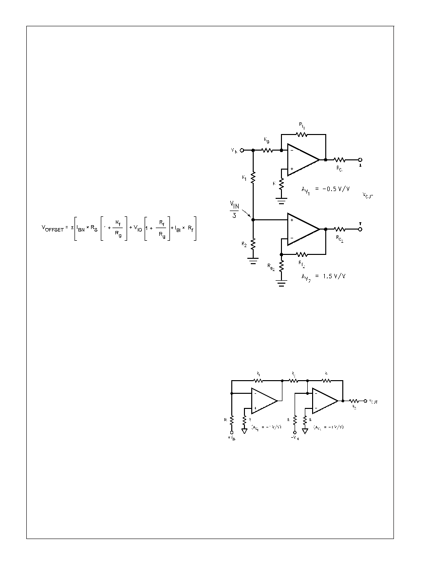
FIGURE 3. Single-to-Differential Line Driver
20088546
FIGURE 4. Differential Line Receiver
LMH6715EP
Enhanced
Plastic
www.national.com
11
相关PDF资料 |
PDF描述 |
|---|---|
| LMH6720J-QML/NOPB | 1 CHANNEL, VIDEO AMPLIFIER, CDIP8 |
| 5962-0420301QPA | 1 CHANNEL, VIDEO AMPLIFIER, CDIP8 |
| 5962-0420301QZA | 1 CHANNEL, VIDEO AMPLIFIER, CDSO8 |
| LMH6720WG-QML/NOPB | 1 CHANNEL, VIDEO AMPLIFIER, CDSO8 |
| LMH6722J-QML/NOPB | 1 CHANNEL, VIDEO AMPLIFIER, CDIP14 |
相关代理商/技术参数 |
参数描述 |
|---|---|
| LMH6718 | 制造商:NSC 制造商全称:National Semiconductor 功能描述:Dual, High Output, Programmable Gain Buffer |
| LMH6718IMAX | 制造商:NSC 制造商全称:National Semiconductor 功能描述:Dual, High Output, Programmable Gain Buffer |
| LMH6718MA | 制造商:Texas Instruments 功能描述:AMP BUFFER DUAL HIGH O/P SMD 6718 |
| LMH6718MA/NOPB | 功能描述:BUFFER PROG DUAL HI OUT 8-SOIC RoHS:是 类别:集成电路 (IC) >> Linear - Amplifiers - Instrumentation 系列:VIP10™ 标准包装:1,000 系列:- 放大器类型:电压反馈 电路数:4 输出类型:满摆幅 转换速率:33 V/µs 增益带宽积:20MHz -3db带宽:30MHz 电流 - 输入偏压:2nA 电压 - 输入偏移:3000µV 电流 - 电源:2.5mA 电流 - 输出 / 通道:30mA 电压 - 电源,单路/双路(±):4.5 V ~ 16.5 V,±2.25 V ~ 8.25 V 工作温度:-40°C ~ 85°C 安装类型:表面贴装 封装/外壳:14-SOIC(0.154",3.90mm 宽) 供应商设备封装:14-SOIC 包装:带卷 (TR) |
| LMH6718MAX/NOPB | 功能描述:IC BUFFER SELECT GAIN DUAL 8SOIC RoHS:是 类别:集成电路 (IC) >> Linear - Amplifiers - Instrumentation 系列:VIP10™ 其它有关文件:Automotive Product Guide 产品培训模块:Lead (SnPb) Finish for COTS Obsolescence Mitigation Program 标准包装:1 系列:- 放大器类型:通用 电路数:1 输出类型:满摆幅 转换速率:3 V/µs 增益带宽积:10MHz -3db带宽:- 电流 - 输入偏压:1pA 电压 - 输入偏移:70µV 电流 - 电源:2.5mA 电流 - 输出 / 通道:48mA 电压 - 电源,单路/双路(±):2.7 V ~ 5.5 V,±1.35 V ~ 2.75 V 工作温度:-40°C ~ 125°C 安装类型:表面贴装 封装/外壳:SOT-23-6 供应商设备封装:SOT-6 包装:Digi-Reel® 其它名称:MAX4475AUT#TG16DKR |
发布紧急采购,3分钟左右您将得到回复。