- 您现在的位置:买卖IC网 > PDF目录358884 > LMV242LD (NATIONAL SEMICONDUCTOR CORP) Dual Output, Quad-Band GSM/GPRS Power Amplifier Controller PDF资料下载
参数资料
| 型号: | LMV242LD |
| 厂商: | NATIONAL SEMICONDUCTOR CORP |
| 元件分类: | 通信及网络 |
| 英文描述: | Dual Output, Quad-Band GSM/GPRS Power Amplifier Controller |
| 中文描述: | SPECIALTY TELECOM CIRCUIT, DSO10 |
| 封装: | 3 X 3 MM, LLP-10 |
| 文件页数: | 12/16页 |
| 文件大小: | 560K |
| 代理商: | LMV242LD |
Application Section
(Continued)
We will assume initially that the output of the PA is at some
low level and that the V
RAMP
voltage is at 1V. The V/I
converter converts the V
RAMP
voltage to a sinking current
I
RAMP
. This current can only come from the integrator ca-
pacitor C. Current flow from this direction increases the
output voltage of the integrator. The output voltage, which
drives the V
of the PA, increases the gain (we assume
that the PA’s gain control input has a positive sense, that is,
increasing voltage increases gain). The gain will increase,
thereby increasing the amplifier’s output level until the de-
tector output current equals the ramp current I
. At that
point, the current through the capacitor will decrease to zero
and the integrator output will be held constant, thereby set-
tling the loop. If capacitor charge is lost over time, output
voltage will decrease. However, this leakage will quickly be
corrected by additional current from the detector. The loop
stabilizes to I
DET
= I
RAMP
thereby creating a direct relation
between the V
independent of the PA’s V
APC
-P
OUT
characteristics.
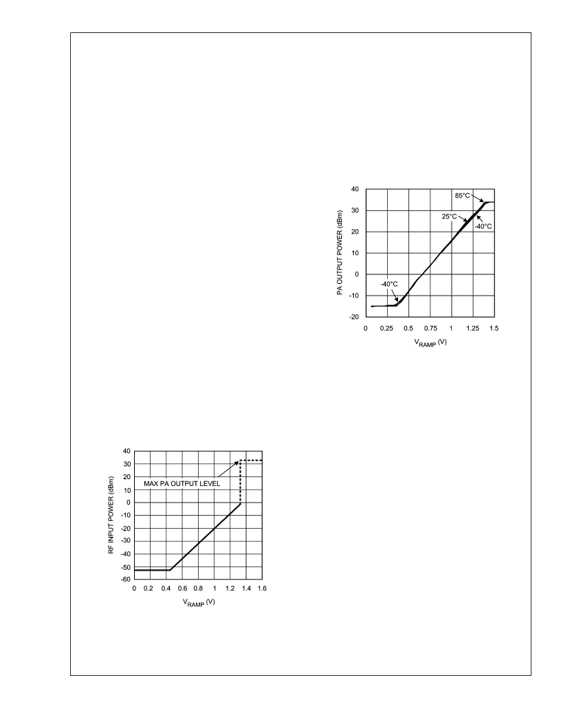
Power Control Over Wide Dynamic Range
The circuit as described so far, has been designed to pro-
duce a temperature independent output power level. If the
detector has a high dynamic range, the circuit can precisely
set PA output levels over a wide power range. To set a PA
output power level, the reference voltage, V
RAMP
, is varied.
To estimate the response of P
OUT
vs. V
RAMP
, P
IN
vs. V
RAMP
of the LMV242 should be known (P
OUT
= P
IN
+ attenuation
as discussed is section 3).
The relation between P
IN
and V
RAMP
can be constructed out
of 2 curves:
I
COMP
vs, V
RAMP
V
OUT
vs. RF Input Power (detection curve)
I
can be calculated by dividing the V
of the detection
curve by the feedback resistor used for measuring. With the
knowledge that I
COMP
= I
in a closed loop the resulting
function P
vs. V
is shown in
Figure 2
. Extra attenua-
tion should be inserted between PA output and LMV242’s
P
IN
to match their dynamic ranges.
Using a closed loop to control the PA has benefits over the
use of a directly controlled PA. Non-linearity’s and tempera-
ture variations present in the PA transfer function do not
appear in the overall transfer function, P
vs. V
The
response of a typical closed loop is given in
Figure 3
. The
shape of this curve is determined by the response of the
controller’s detector. Therefore the detector needs to be
accurate, temperature stable and preferably linear in dB to
achieve a accurately controlled output power. The only re-
quirement for the control loop is that the gain control function
of the PA has to be monotonic. With a linear in dB detector,
the relation between V
RAMP
and PA output power becomes
linear in dB as well, which makes calibration of the system
easy.
The response time of the loop can be controlled by varying
the RC time constant of the integrator. Setting this at a low
level will result in fast output settling but can result in ringing
in the output envelope. Setting the RC time constant to a
high value will give the loop good stability but will increase
settling time.
ATTENUATION BETWEEN COUPLER AND LMV242
DETECTOR
Figure 4
shows a practical RF power control loop realized by
using the National’s LMV242 with integrated RF detector.
The RF signal from the PA passes through a directional
coupler on its way to the antenna. Directional couplers are
characterized by their coupling factor, which is in the 10 dB
to 30 dB range, typical 20 dB. Because the coupled output
must in its own right deliver some power (in this case to the
detector), the coupling process takes some power from the
main output. This manifests itself as insertion loss, the inser-
tion loss being higher for lower coupling factors.
It is very important to choose the right attenuation between
PA output and detector input to achieve power control over
the full output power range of the PA. A typical value for the
output power of the PA is +35.5 dBm for GSM and +30 dBm
for PCS/DCS. In order to accommodate these levels into the
LMV242 detection range the minimum required total attenu-
ation is about 35 dBm (please refer to typical performance
characteristics in the datasheet and
Figure 2
). A typical
coupler factor is 20 dB. An extra attenuation of about 15 dB
should be inserted.
20079521
FIGURE 2. P
IN
vs. V
RAMP
20079522
FIGURE 3. Closed Loop Response
L
www.national.com
12
相关PDF资料 |
PDF描述 |
|---|---|
| LMV242MWA | Dual Output, Quad-Band GSM/GPRS Power Amplifier Controller |
| LMV242LDX | Silver Mica Capacitor; Capacitance:510pF; Capacitance Tolerance: 5%; Series:CDV30; Voltage Rating:1500VDC; Capacitor Dielectric Material:Mica; Termination:Radial Leaded; Lead Pitch:11.1mm; Leaded Process Compatible:No RoHS Compliant: No |
| LMV242 | Dual Output, Quad-Band GSM/GPRS Power Amplifier Controller |
| LMV301 | Low Input Bias Current, 1.8V Op Amp w/ Rail-to-Rail Output |
| LMV301MG | Low Input Bias Current, 1.8V Op Amp w/ Rail-to-Rail Output |
相关代理商/技术参数 |
参数描述 |
|---|---|
| LMV242LD/NOPB | 功能描述:射频检测器 RoHS:否 制造商:Skyworks Solutions, Inc. 配置: 频率范围:650 MHz to 3 GHz 最大二极管电容: 最大工作温度:+ 85 C 最小工作温度:- 40 C 封装 / 箱体:SC-88 封装:Reel |
| LMV242LDX | 功能描述:射频检测器 RoHS:否 制造商:Skyworks Solutions, Inc. 配置: 频率范围:650 MHz to 3 GHz 最大二极管电容: 最大工作温度:+ 85 C 最小工作温度:- 40 C 封装 / 箱体:SC-88 封装:Reel |
| LMV242LDX/NOPB | 功能描述:射频检测器 RoHS:否 制造商:Skyworks Solutions, Inc. 配置: 频率范围:650 MHz to 3 GHz 最大二极管电容: 最大工作温度:+ 85 C 最小工作温度:- 40 C 封装 / 箱体:SC-88 封装:Reel |
| LMV242MDA | 制造商:NSC 制造商全称:National Semiconductor 功能描述:Dual Output, Quad-Band GSM/GPRS Power Amplifier Controller |
| LMV242MEA DIE | 制造商:Texas Instruments 功能描述: |
发布紧急采购,3分钟左右您将得到回复。