- 您现在的位置:买卖IC网 > PDF目录358884 > LMV242LDX (NATIONAL SEMICONDUCTOR CORP) Silver Mica Capacitor; Capacitance:510pF; Capacitance Tolerance: 5%; Series:CDV30; Voltage Rating:1500VDC; Capacitor Dielectric Material:Mica; Termination:Radial Leaded; Lead Pitch:11.1mm; Leaded Process Compatible:No RoHS Compliant: No PDF资料下载
参数资料
| 型号: | LMV242LDX |
| 厂商: | NATIONAL SEMICONDUCTOR CORP |
| 元件分类: | 通信及网络 |
| 英文描述: | Silver Mica Capacitor; Capacitance:510pF; Capacitance Tolerance: 5%; Series:CDV30; Voltage Rating:1500VDC; Capacitor Dielectric Material:Mica; Termination:Radial Leaded; Lead Pitch:11.1mm; Leaded Process Compatible:No RoHS Compliant: No |
| 中文描述: | SPECIALTY TELECOM CIRCUIT, DSO10 |
| 封装: | 3 X 3 MM, LLP-10 |
| 文件页数: | 4/16页 |
| 文件大小: | 560K |
| 代理商: | LMV242LDX |
5.0V Electrical Characteristics
Unless otherwise specified, all limits are guaranteed to T
J
= 25C.
V
DD
= 5.0V.
Boldface
limits apply at temperature extremes (Note 4). (Continued)
Symbol
Error Amplifier
GBW
V
O
Parameter
Condition
Min
Typ
Max
Units
Gain-Bandwidth Product
Output Swing from Rail
(Note 8)
From Positive Rail, Sourcing,
I
O
= 7 mA
From Negative Rail Sinking,
I
O
= 7 mA
Sourcing, V
O
= 4.8V
Sinking, V
O
= 0.2V
f
MEASURE
= 10 kHz,
RF Input = 1800 MHz,
-10dBm, 20 k
// 68 pF
between V
COMP1
and V
COMP2
,
V
OUT
= 1.4V, set by V
RAMP
,
(Note 8)
5.7
31
MHz
80
105
80
105
mV
35
I
O
Output Short Circuit Current
(Note 3)
15
15
31.5
31.5
770
mA
e
n
Output Referred Noise
nV/
SR
Slew Rate
2.5
4.9
V/μs
Note 1:
Absolute Maximum Ratings indicate limits beyond which damage to the device may occur. Operating Ratings indicate conditions for which the device is
intended to be functional, but specific performance is not guaranteed. For guaranteed specifications and the test conditions, see the Electrical Characteristics.
Note 2:
Human body model: 1.5 k
in series with 100 pF.
Note 3:
The output is not short circuit protected internally. External protection is necessary to prevent overheating and destruction or adverse reliability.
Note 4:
Electrical Table values apply only for factory testing conditions at the temperature indicated. Factory testing conditions result in very limited self-heating of
the device such that T
J
= T
A
. No guarantee of parametric performance is indicated in the electrical tables under conditions of internal self-heating where T
J
>
T
A
.
Note 5:
Power in dBV = dBm + 13 when the impedance is 50
.
Note 6:
The maximum power dissipation is a function of T
J(MAX)
,
θ
JA
and T
A
. The maximum allowable power dissipation at any ambient temperature is P
D
=
(T
J(MAX)
- T
A
)/
θ
JA
. All numbers apply for packages soldered directly into a PC board.
Note 7:
All limits are guaranteed by design or statistical analysis.
Note 8:
Typical values represent the most likely parametric norm.
Note 9:
Slope and intercept are calculated from graphs "V
OUT
vs. RF input power" where the current is obtained by division of the voltage by 20 k
.
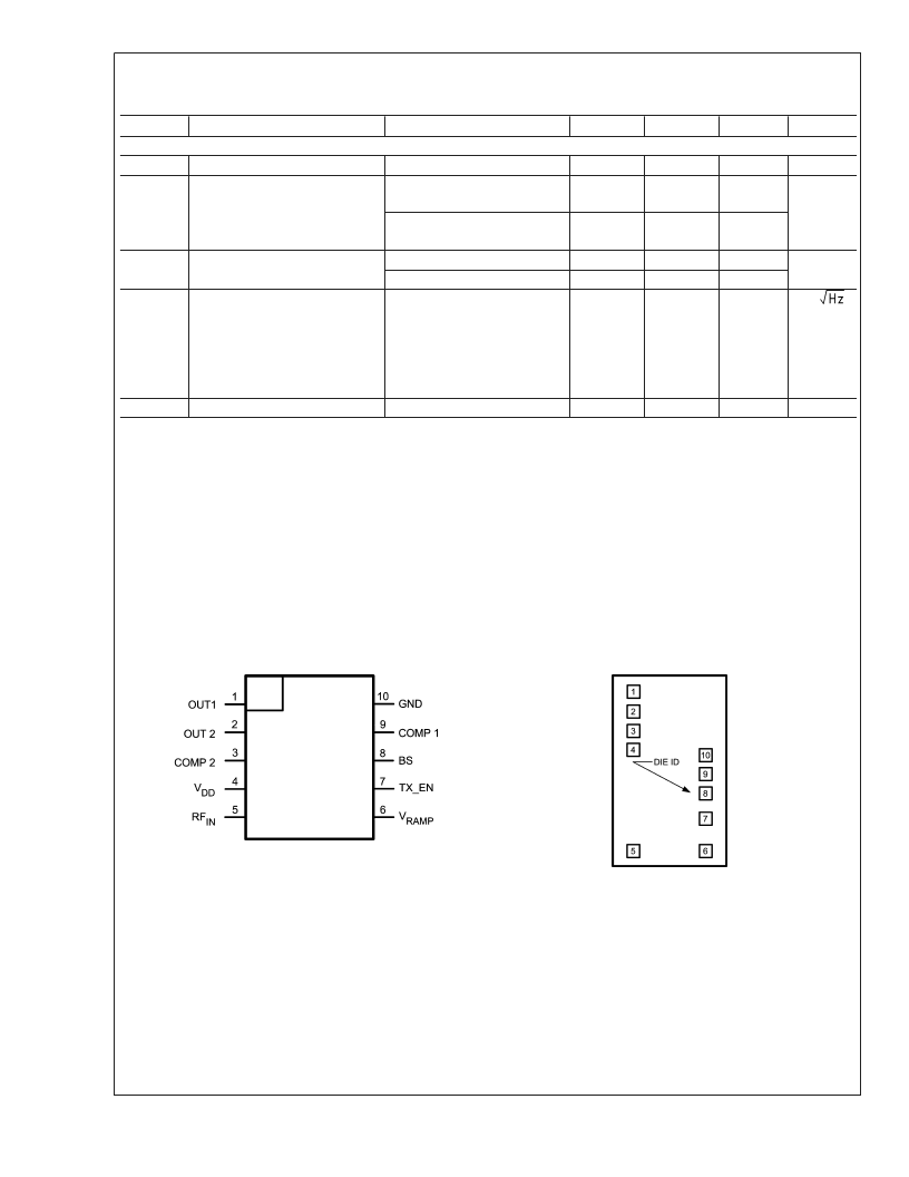
Connection Diagrams
LLP-10
Bond Pad Layout
20079502
Top View
20079503
Top View
L
www.national.com
4
相关PDF资料 |
PDF描述 |
|---|---|
| LMV242 | Dual Output, Quad-Band GSM/GPRS Power Amplifier Controller |
| LMV301 | Low Input Bias Current, 1.8V Op Amp w/ Rail-to-Rail Output |
| LMV301MG | Low Input Bias Current, 1.8V Op Amp w/ Rail-to-Rail Output |
| LMV301MGX | Low Input Bias Current, 1.8V Op Amp w/ Rail-to-Rail Output |
| LMV324D | LOW-VOLTAGE RAIL-TO-RAIL OUTPUT OPERATIONAL AMPLIFIERS |
相关代理商/技术参数 |
参数描述 |
|---|---|
| LMV242LDX/NOPB | 功能描述:射频检测器 RoHS:否 制造商:Skyworks Solutions, Inc. 配置: 频率范围:650 MHz to 3 GHz 最大二极管电容: 最大工作温度:+ 85 C 最小工作温度:- 40 C 封装 / 箱体:SC-88 封装:Reel |
| LMV242MDA | 制造商:NSC 制造商全称:National Semiconductor 功能描述:Dual Output, Quad-Band GSM/GPRS Power Amplifier Controller |
| LMV242MEA DIE | 制造商:Texas Instruments 功能描述: |
| LMV242MWA | 制造商:NSC 制造商全称:National Semiconductor 功能描述:Dual Output, Quad-Band GSM/GPRS Power Amplifier Controller |
| LMV243 | 制造商:NSC 制造商全称:National Semiconductor 功能描述:Single-Channel, Quad-Band GSM Power Controller in micro SMD |
发布紧急采购,3分钟左右您将得到回复。