- 您现在的位置:买卖IC网 > PDF目录358884 > LMV242LDX (NATIONAL SEMICONDUCTOR CORP) Silver Mica Capacitor; Capacitance:510pF; Capacitance Tolerance: 5%; Series:CDV30; Voltage Rating:1500VDC; Capacitor Dielectric Material:Mica; Termination:Radial Leaded; Lead Pitch:11.1mm; Leaded Process Compatible:No RoHS Compliant: No PDF资料下载
参数资料
| 型号: | LMV242LDX |
| 厂商: | NATIONAL SEMICONDUCTOR CORP |
| 元件分类: | 通信及网络 |
| 英文描述: | Silver Mica Capacitor; Capacitance:510pF; Capacitance Tolerance: 5%; Series:CDV30; Voltage Rating:1500VDC; Capacitor Dielectric Material:Mica; Termination:Radial Leaded; Lead Pitch:11.1mm; Leaded Process Compatible:No RoHS Compliant: No |
| 中文描述: | SPECIALTY TELECOM CIRCUIT, DSO10 |
| 封装: | 3 X 3 MM, LLP-10 |
| 文件页数: | 5/16页 |
| 文件大小: | 560K |
| 代理商: | LMV242LDX |
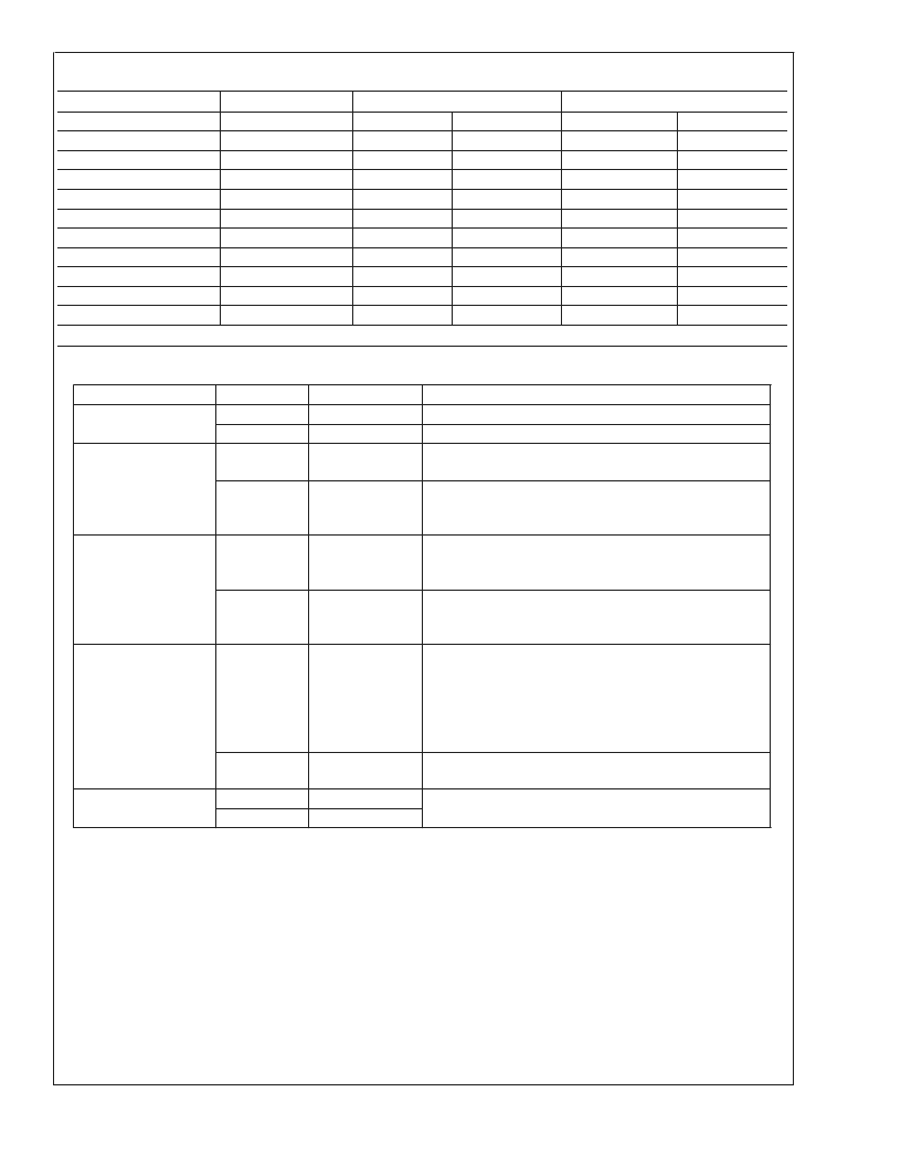
Bond Pad mechanical Dimensions
X/Y Coordinates
Pad Size
Signal Name
Out 1
Out 2
Comp2
V
DD
RF
IN
V
RAMP
TX_EN
BS
Comp1
GND
Pad Number
1
2
3
4
5
6
7
8
9
10
X
Y
X
92
92
92
92
92
92
92
92
92
92
Y
92
92
92
92
92
92
92
92
92
92
281
281
281
281
281
281
281
281
281
281
617
490
363
236
617
617
360
118
20
187
Note:
Dimensions of the bond pad coordinates are in μm Origin of the coordinates: center of the die Coordinates refer to the center of the bond pad
Pin Descriptions
Pin
4
10
7
Name
V
DD
GND
TX_EN
Description
Positive Supply Voltage
Power Ground
Schmitt-triggered logic input. A LOW shuts down the whole
chip for battery saving purposes. A HIGH enables the chip.
Schmitt-triggered Band Select pin. When BS = H, channel 1
(OUT1) is selected, when BS = L, channel 2 (OUT2) is
selected.
RF Input connected to the Coupler output with optional
attenuation to measure the Power Amplifier (PA) / Antenna
RF power levels.
Sets the RF output power level. The useful input voltage
range is from 0.2V to 1.8V, although voltages from 0V to V
DD
are allowed.
Connects an external RC network between the Comp1 pin
and the Comp2 pin for an overall loop compensation and to
control the closed loop frequency response. Conventional
loop stability techniques can be used in selecting this
network, such as Bode plots. A good starting value for the
RC combination will be C = 68 pF and R = 0
.
Frequency compensation pin. The BS signal switches this pin
either to OUT1 or to OUT2.
This pin is connected to the PA of either channel 1 or
channel 2.
Power Supply
Digital Inputs
8
BS
Analog Inputs
5
RF
IN
6
V
RAMP
Compensation
9
Comp1
3
Comp2
Output
1
2
Out1
Out2
Note:
1. All inputs and outputs are referenced to GND (pin 10).
2. For the digital inputs, a LOW is
<
0.8V and a HIGH is
>
1.8V.
3. RF power detection is performed internally in the LMV242 and only an RF power coupler with optional extra attenuation has to be used.
L
www.national.com
5
相关PDF资料 |
PDF描述 |
|---|---|
| LMV242 | Dual Output, Quad-Band GSM/GPRS Power Amplifier Controller |
| LMV301 | Low Input Bias Current, 1.8V Op Amp w/ Rail-to-Rail Output |
| LMV301MG | Low Input Bias Current, 1.8V Op Amp w/ Rail-to-Rail Output |
| LMV301MGX | Low Input Bias Current, 1.8V Op Amp w/ Rail-to-Rail Output |
| LMV324D | LOW-VOLTAGE RAIL-TO-RAIL OUTPUT OPERATIONAL AMPLIFIERS |
相关代理商/技术参数 |
参数描述 |
|---|---|
| LMV242LDX/NOPB | 功能描述:射频检测器 RoHS:否 制造商:Skyworks Solutions, Inc. 配置: 频率范围:650 MHz to 3 GHz 最大二极管电容: 最大工作温度:+ 85 C 最小工作温度:- 40 C 封装 / 箱体:SC-88 封装:Reel |
| LMV242MDA | 制造商:NSC 制造商全称:National Semiconductor 功能描述:Dual Output, Quad-Band GSM/GPRS Power Amplifier Controller |
| LMV242MEA DIE | 制造商:Texas Instruments 功能描述: |
| LMV242MWA | 制造商:NSC 制造商全称:National Semiconductor 功能描述:Dual Output, Quad-Band GSM/GPRS Power Amplifier Controller |
| LMV243 | 制造商:NSC 制造商全称:National Semiconductor 功能描述:Single-Channel, Quad-Band GSM Power Controller in micro SMD |
发布紧急采购,3分钟左右您将得到回复。