- 您现在的位置:买卖IC网 > PDF目录2153 > LMV324AMTC14X (Fairchild Semiconductor)IC AMP R-R OUT QUAD LV 14-TSSOP PDF资料下载
参数资料
| 型号: | LMV324AMTC14X |
| 厂商: | Fairchild Semiconductor |
| 文件页数: | 14/16页 |
| 文件大小: | 0K |
| 描述: | IC AMP R-R OUT QUAD LV 14-TSSOP |
| 标准包装: | 2,500 |
| 放大器类型: | 电压反馈 |
| 电路数: | 4 |
| 输出类型: | 满摆幅 |
| 转换速率: | 1.5 V/µs |
| 增益带宽积: | 1.4MHz |
| 电流 - 输入偏压: | 1nA |
| 电压 - 输入偏移: | 1000µV |
| 电流 - 电源: | 100µA |
| 电流 - 输出 / 通道: | 34mA |
| 电压 - 电源,单路/双路(±): | 2.7 V ~ 5.5 V,±1.35 V ~ 2.75 V |
| 工作温度: | -40°C ~ 125°C |
| 安装类型: | 表面贴装 |
| 封装/外壳: | 14-TSSOP(0.173",4.40mm 宽) |
| 供应商设备封装: | 14-TSSOP |
| 包装: | 带卷 (TR) |
LMV321/LMV358/LMV324
DATA SHEET
REV. 1D. Feb. 2012
7
Application Information
General Description
voltage-feedback amplifiers that are pin-for-pin compatible
and drop in replacements with other industry standard
LMV321, LMV358, and LMV324 amplifiers. The LMV3XX
family is fabricated on a CMOS process, features a rail-to-rail
output, and is unity gain stable.
The typical non-inverting circuit schematic is shown in Figure
1.
Figure 1: Typical Non-inverting configuration
Power Dissipation
The maximum internal power dissipation allowed is directly
related to the maximum junction temperature. If the maximum
junction temperature exceeds 150°C, some performance
degradation will occur. If the maximum junction temperature
exceeds 175°C for an extended time, device failure may occur.
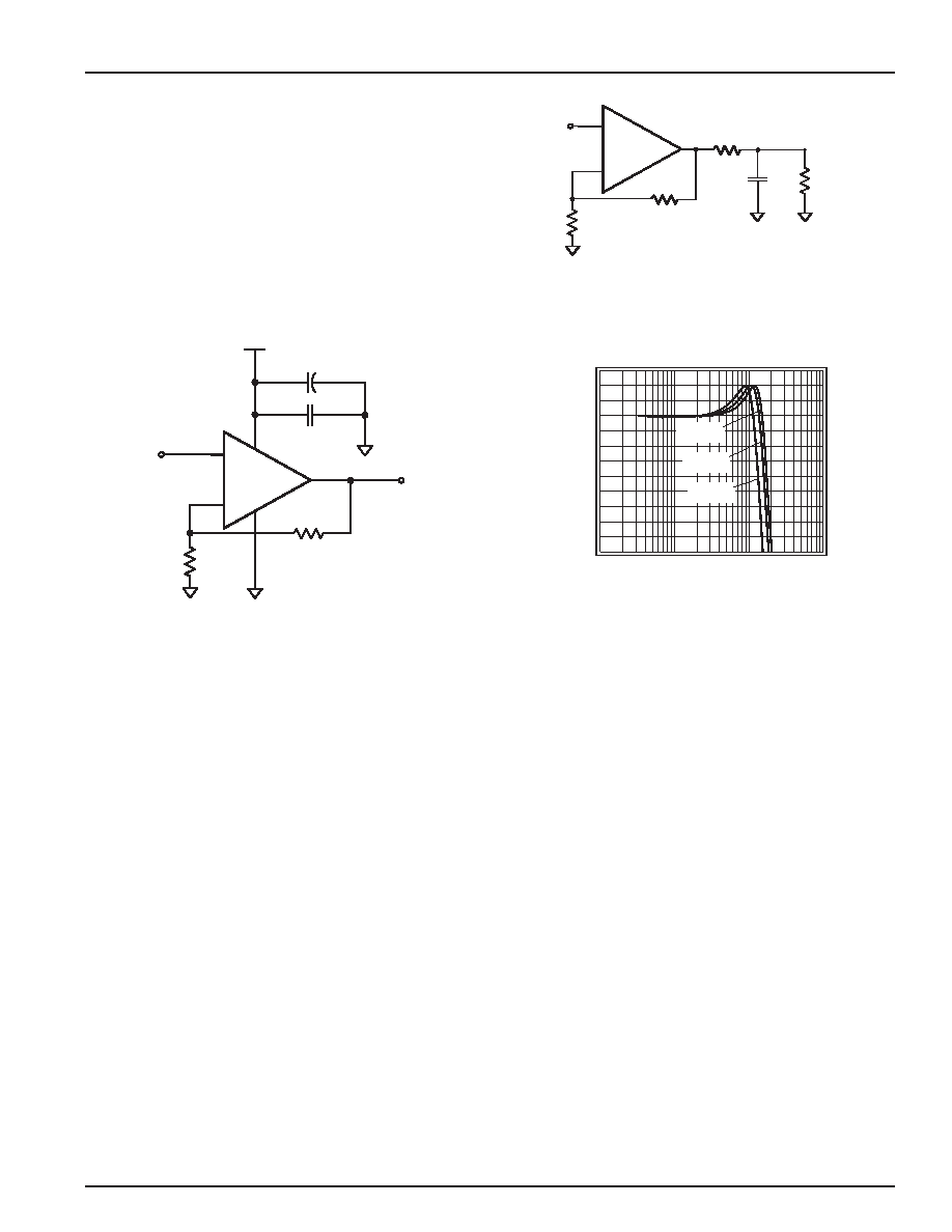
Driving Capacitive Loads
The Frequency Response vs CL plot on page 4, illustrates the
response of the LMV3XX family. A small series resistance (Rs)
at the output of the amplifier, illustrated in Figure 2, will improve
stability and settling performance. Rs values in the Frequency
Response vs CL plot were chosen to achieve maximum band-
width with less than 1dB of peaking. For maximum flatness,
use a larger Rs. As the plot indicates, the LMV3XX family
can easily drive a 200pF capacitive load without a series
resistance. For comparison, the plot also shows the LMV321
driving a 200pF load with a 225
series resistance.
Driving a capacitive load introduces phase-lag into the output
signal, which reduces phase margin in the amplifier. The
unity gain follower is the most sensitive configuration. In a
unity gain follower configuration, the LMV3XX family
requires a 450
series resistor to drive a 200pF load. The
response is illustrated in Figure 3.
Figure 2: Typical Topology for driving a
capacitive load
Figure 3: Frequency Response vs CL for unity
gain configuration
Layout Considerations
General layout and supply bypassing play major roles in high
frequency performance. Fairchild has evaluation boards to
use as a guide for high frequency layout and as aid in device
testing and characterization. Follow the steps below as a
basis for high frequency layout:
Include 6.8
F and 0.01F ceramic capacitors
Place the 6.8
F capacitor within 0.75 inches of
the power pin
Place the 0.01
F capacitor within 0.1 inches of
the power pin
Remove the ground plane under and around the part,
especially near the input and output pins to reduce
parasitic capacitance
Minimize all trace lengths to reduce series inductances
Refer to the evaluation board layouts shown in Figure 5 on
page 8 for more information.
+
-
LMV3XX
Rf
0.01
F
6.8
F
Out
+In
+Vs
+
Rg
+
-
10k
10k
Rs
CL
2k
LMV3XX
Magnitude
(
dB
)
Frequency (M H z )
0.01
0.1
1
10
-9
-8
-7
-6
-5
-4
-3
-2
-1
0
1
2
3
CL = 50pF
Rs = 0
CL = 100pF
Rs = 400
CL = 200pF
Rs = 450
The LMV3XX family are dual supply, general purpose,
相关PDF资料 |
PDF描述 |
|---|---|
| LMV821SQ3T2G | IC OP AMP SGL LV SC-88A-5 |
| LMV824MT/NOPB | IC OP AMP R-R LOW V LP 14-TSSOP |
| LMV931SQ3T2G | IC OP AMP R-R 1.8V SC-70 |
| LMV982MUTAG | IC OP AMP RRIO DUAL 1.8V 10UQFN |
| LMX324ASD+T | IC OP AMP LV R-R QUAD 14-SOIC |
相关代理商/技术参数 |
参数描述 |
|---|---|
| LMV324AMTC14X_Q | 功能描述:运算放大器 - 运放 Low Cost RRO amp General Purpose Quad RoHS:否 制造商:STMicroelectronics 通道数量:4 共模抑制比(最小值):63 dB 输入补偿电压:1 mV 输入偏流(最大值):10 pA 工作电源电压:2.7 V to 5.5 V 安装风格:SMD/SMT 封装 / 箱体:QFN-16 转换速度:0.89 V/us 关闭:No 输出电流:55 mA 最大工作温度:+ 125 C 封装:Reel |
| LMV324BG-13 | 功能描述:运算放大器 - 运放 OpAmp General Purpos SO-14,2.5K RoHS:否 制造商:STMicroelectronics 通道数量:4 共模抑制比(最小值):63 dB 输入补偿电压:1 mV 输入偏流(最大值):10 pA 工作电源电压:2.7 V to 5.5 V 安装风格:SMD/SMT 封装 / 箱体:QFN-16 转换速度:0.89 V/us 关闭:No 输出电流:55 mA 最大工作温度:+ 125 C 封装:Reel |
| LMV324BG-7 | 制造商:DIODES 制造商全称:Diodes Incorporated 功能描述:GENERAL PURPOSE, LOW VOLTAGE, RAIL-TO-RAIL |
| LMV324D | 制造商:TI 制造商全称:Texas Instruments 功能描述:LOW-VOLTAGE RAIL-TO-RAIL OUTPUT OPERATIONAL AMPLIFIERS |
| LMV324DR2G | 功能描述:运算放大器 - 运放 LV R2R OPAMPK RoHS:否 制造商:STMicroelectronics 通道数量:4 共模抑制比(最小值):63 dB 输入补偿电压:1 mV 输入偏流(最大值):10 pA 工作电源电压:2.7 V to 5.5 V 安装风格:SMD/SMT 封装 / 箱体:QFN-16 转换速度:0.89 V/us 关闭:No 输出电流:55 mA 最大工作温度:+ 125 C 封装:Reel |
发布紧急采购,3分钟左右您将得到回复。