- 您现在的位置:买卖IC网 > PDF目录358886 > LMX2312U (NATIONAL SEMICONDUCTOR CORP) PLLatinum⑩ Ultra Low Power Frequency Synthesizer for RF Personal Communications PDF资料下载
参数资料
| 型号: | LMX2312U |
| 厂商: | NATIONAL SEMICONDUCTOR CORP |
| 元件分类: | XO, clock |
| 英文描述: | PLLatinum⑩ Ultra Low Power Frequency Synthesizer for RF Personal Communications |
| 中文描述: | PLL FREQUENCY SYNTHESIZER, 1200 MHz, QCC20 |
| 封装: | THIN, CSP-20 |
| 文件页数: | 23/29页 |
| 文件大小: | 662K |
| 代理商: | LMX2312U |
第1页第2页第3页第4页第5页第6页第7页第8页第9页第10页第11页第12页第13页第14页第15页第16页第17页第18页第19页第20页第21页第22页当前第23页第24页第25页第26页第27页第28页第29页
1.0 Functional Description
(Continued)
1.5 PHASE/FREQUENCY DETECTORS
The phase/frequency detector is driven from the N and R
COUNTER outputs. The maximum frequency at the phase
detector inputs is 10 MHz. The phase detector outputs con-
trol the charge pump. The polarity of the pump-up or pump-
down control signals are programmed using the PD_POL
control bit, depending on whether the RF VCO tuning char-
acteristics are positive or negative (see programming de-
scription in Section 3.2.2). The phase/frequency detector
has a detection range of 2
π
to +2
π
.
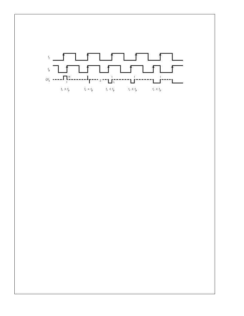
Phase Comparator and Internal Charge Pump Characteristics
20043804
Note 13:
The minimum width of the pump up and pump down current pulses occur at the CP
o
pin when the loop is phase-locked.
Note 14:
The diagram assumes that PD_POL = 1
Note 15:
f
r
is the phase comparator input from the R Divider
Note 16:
f
p
is the phase comparator input from the N Divider
Note 17:
CP
o
is charge pump output
1.6 CHARGE PUMP
The charge pumps directs charge into or out of an external
loop filter. The loop filter converts the charge into a stable
control voltage which is applied to the tuning input of a VCO.
The charge pump steers the VCO control voltage towards V
P
during pump-up events and towards GND during pump-
down events. When locked, CP
is primarily in a TRI-STATE
condition with small corrections occurring at the phase com-
parison rate. The charge pump output current magnitude can
be selected as 1.0 mA or 4.0 mA by programming the
ICPo_4X bits. When TO_CNTR[11:0] = 1, the charge pump
output current magnitude is set to 4.0 mA. Refer to Section
3.2.3 and 3.4.2 for details on programming the charge pump
output current magnitude.
1.7 MICROWIRE SERIAL INTERFACE
The programmable register set is accessed through the
MICROWIRE serial interface. The interface is comprised of
three signal pins: CLOCK, DATA and LE (Latch Enable). The
MICROWIRE circuitry is referenced to V
μC
, which allows the
circuitry to operate down to a 1.72V source. Serial data is
clocked into a 22-bit shift register from DATA on the rising
edge of CLOCK. The serial data is clocked in MSB first. The
last two bits decode the internal register address. On the
rising edge of LE, the data stored in the shift register is
loaded into one of the three latches based on the address
bits. The synthesizer can be programmed even in the power-
down state. A complete programming description is in Sec-
tion 3.0.
1.8 MULTI-FUNCTION OUTPUTS
The LMX2310/1/2/3U FoLD output pin is a multi-function
output that can be configured as an analog lock detect, a
digital lock detect, and a monitor of the output of the refer-
ence divider and the feedback divider circuits. The FoLD
output pin is referenced to the V
supply. The FoLD0,
FoLD1 and FoLD2 bits are used to select the desired output
function. A complete programming description of the FoLD
output pin is in Section 3.2.5.
1.8.1 Analog Lock Detect
When programmed for analog lock detect, the analog lock
detect status is available on the FoLD output pin. When the
charge pump is inactive, the lock detect output goes to a
high impedance in the open drain configuration and to a V
source in a push-pull configuration. It goes low when the
charge pump is active during a comparison cycle. The ana-
log lock detect status can be programmed in either an open
drain or push-pull configuration. The push-pull output is ref-
erenced to V
μC
.
1.8.2 Digital Lock Detect
When programmed for digital lock detect, the digital lock
detect status is available on the FoLD pin. The digital lock
detect filter compares the phase difference of the inputs from
the phase detector to a RC generated delay of approxi-
mately 15 ns. To enter the locked state (LD = High), the
phase error must be less than the 15 ns RC delay for 5
consecutive reference cycles. Once in lock, the RC delay is
changed to approximately 30 ns. To exit the locked state, the
phase error must be greater than the 30 ns RC delay. When
a PLL is in power-down mode, the respective lock detect
output is always low. A flow chart of the digital lock detect
filter follows:
L
www.national.com
23
相关PDF资料 |
PDF描述 |
|---|---|
| LMX2314 | 1.2 GHz Frequency Synthesizer for RF Personal Communications |
| LMX2314M | 1.2 GHz Frequency Synthesizer for RF Personal Communications |
| LMX2314MX | 1.2 GHz Frequency Synthesizer for RF Personal Communications |
| LMX2315 | Frequency Synthesizer for RF Personal Communications |
| LMX2315TM | Frequency Synthesizer for RF Personal Communications |
相关代理商/技术参数 |
参数描述 |
|---|---|
| LMX2312USLDX | 制造商:MAJOR 功能描述: |
| LMX2312USLDX/NOPB | 功能描述:IC FREQ SYNTH 1.2GHZ 20LAMTCSP RoHS:是 类别:集成电路 (IC) >> 时钟/计时 - 时钟发生器,PLL,频率合成器 系列:PLLatinum™ 标准包装:39 系列:- 类型:* PLL:带旁路 输入:时钟 输出:时钟 电路数:1 比率 - 输入:输出:1:10 差分 - 输入:输出:是/是 频率 - 最大:170MHz 除法器/乘法器:无/无 电源电压:2.375 V ~ 3.465 V 工作温度:0°C ~ 70°C 安装类型:* 封装/外壳:* 供应商设备封装:* 包装:* |
| LMX2313U | 制造商:NSC 制造商全称:National Semiconductor 功能描述:PLLatinum⑩ Ultra Low Power Frequency Synthesizer for RF Personal Communications |
| LMX2313USLDX | 制造商:NSC 制造商全称:National Semiconductor 功能描述:PLLatinum⑩ Ultra Low Power Frequency Synthesizer for RF Personal Communications |
| LMX2313USLDX/NOPB | 功能描述:IC FREQ SYNTH 600MHZ 20LAMTCSP RoHS:否 类别:集成电路 (IC) >> 时钟/计时 - 时钟发生器,PLL,频率合成器 系列:PLLatinum™ 标准包装:39 系列:- 类型:* PLL:带旁路 输入:时钟 输出:时钟 电路数:1 比率 - 输入:输出:1:10 差分 - 输入:输出:是/是 频率 - 最大:170MHz 除法器/乘法器:无/无 电源电压:2.375 V ~ 3.465 V 工作温度:0°C ~ 70°C 安装类型:* 封装/外壳:* 供应商设备封装:* 包装:* |
发布紧急采购,3分钟左右您将得到回复。