- 您现在的位置:买卖IC网 > PDF目录358886 > LMX2353TM (NATIONAL SEMICONDUCTOR CORP) PLLatinum⑩ Fractional N Single 2.5 GHz Frequency Synthesizer PDF资料下载
参数资料
| 型号: | LMX2353TM |
| 厂商: | NATIONAL SEMICONDUCTOR CORP |
| 元件分类: | XO, clock |
| 英文描述: | PLLatinum⑩ Fractional N Single 2.5 GHz Frequency Synthesizer |
| 中文描述: | PHASE LOCKED LOOP, 2500 MHz, PDSO16 |
| 封装: | PLASTIC, TSSOP-16 |
| 文件页数: | 13/16页 |
| 文件大小: | 210K |
| 代理商: | LMX2353TM |
2.0 Programming Description
(Continued)
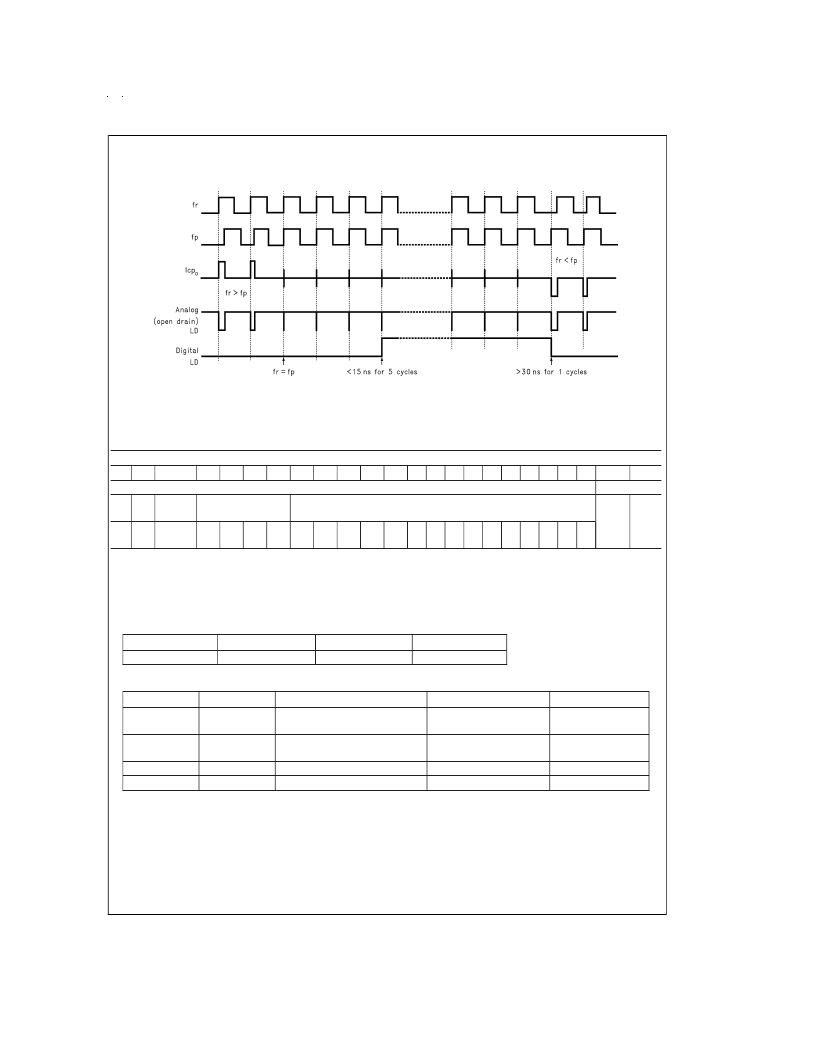
2.4.2.4 Typical Lock Detecting Timing
2.5 F2 REGISTER
If theADDRESS[1:0] field is set to 0 1, data is transferred from the 24-bit shift register into the F2 register when Latch Enable (LE)
signal goes high. The F2 register sets the CMOS output word bit CMOS[3:0] and the power down mode bit PWDN_MODE. The
rest of the bits F2_0 - F2_14, and F2_20-F_21 are Don’t Care.
Most Significant Bit
23
22
SHIFT REGISTER BIT LOCATION
14
13
12
11
Data Field
Least Significant Bit
3
2
1
Address Field
21
20
19
18
17
16
15
10
9
8
7
6
5
4
0
0
0
PWDN_
MODE
F2
_19
CMOS[3:0]
These bits should be set to zero
0
0
F2
_21
F2
_20
F2
_18
F2
_17
F2
_16
F2
_15
F2
_14
F2
_13
F2
_12
F2
_11
F2
_10
F2
_9
F2
_8
F2
_7
F2
_6
F2
_5
F2
_4
F2
_3
F2
_2
F2
_1
F2
_0
Note:
0 denotes setting the bit to zero
2.5.1 PWDN_MODE
See section 2.3.2 describing the control word and power down.
(F2_19)
2.5.2 Programmable CMOS Outputs
(F2_15–F2_18)
F2_18
FastLock
F2_17
TEST
F2_16
OUT_1
F2_15
OUT_0
2.5.3 OUT0/OUT1 Truth Table
Bit
Location
Function
0
1
OUT_0
F2_15
Set the output logic level of
OUT0 pin
Set the output logic level of
OUT1 pin
Test
FastLock Mode
LOW
HIGH
OUT_1
F2_16
LOW
HIGH
TEST
FastLock
The CMOS[3:0] 4-bit register selects one of three modes for the OUT_0 and OUT_1 pins. The OUT_0 and OUT_1 pins are nor-
mally used as general purpose CMOS outputs or as part of a fastlock scheme. There is also a production test mode that overrides
the other two normal modes when activated.
GENERAL PURPOSE CMOS OUTPUT MODE: The general purpose CMOS output mode is selected when the Fastlock bit
(F2_F18) and TEST bit (F2_17) are set LOW. The logic levels of the OUT_0 bit (F2_15) and OUT_1 bit (F2_16) then determine
the logic states of the OUT_0 and OUT_1 pins.
FASTLOCK MODE: The Fastlock bit (F2_18) selects between the general purpose CMOS output or fastlock modes. The fastlock
mode is selected when the fastlock bit is HIGH. The fastlock mode allows the user to open up the loop bandwidth momentarily
while acquiring lock by increasing the charge pump output current magnitude while simultaneously switching in a second resistor
element to ground via the OUT0 output pin.
F2_17
F2_18
Normal Operation
CMOS Output Mode
Test Mode
FastLock Mode
DS101124-7
www.national.com
13
相关PDF资料 |
PDF描述 |
|---|---|
| LMX2353SLBX | PLLatinum⑩ Fractional N Single 2.5 GHz Frequency Synthesizer |
| LMX2353 | PLLatinum⑩ Fractional N Single 2.5 GHz Frequency Synthesizer |
| LMX2372 | PLLatinum⑩ Dual Frequency Synthesizer for RF Personal Communications |
| LMX2372SLBX | PLLatinum⑩ Dual Frequency Synthesizer for RF Personal Communications |
| LMX2372TMX | PLLatinum⑩ Dual Frequency Synthesizer for RF Personal Communications |
相关代理商/技术参数 |
参数描述 |
|---|---|
| LMX2353TM/NOPB | 功能描述:IC FREQ SYNTH 2.5GHZ 16TSSOP RoHS:是 类别:集成电路 (IC) >> 时钟/计时 - 时钟发生器,PLL,频率合成器 系列:PLLatinum™ 标准包装:39 系列:- 类型:* PLL:带旁路 输入:时钟 输出:时钟 电路数:1 比率 - 输入:输出:1:10 差分 - 输入:输出:是/是 频率 - 最大:170MHz 除法器/乘法器:无/无 电源电压:2.375 V ~ 3.465 V 工作温度:0°C ~ 70°C 安装类型:* 封装/外壳:* 供应商设备封装:* 包装:* |
| LMX2353TMX | 制造商:NSC 制造商全称:National Semiconductor 功能描述:PLLatinum⑩ Fractional N Single 2.5 GHz Frequency Synthesizer |
| LMX2353TMX/NOPB | 功能描述:IC FREQ SYNTH 2.5GHZ 16-TSSOP RoHS:是 类别:集成电路 (IC) >> 时钟/计时 - 时钟发生器,PLL,频率合成器 系列:PLLatinum™ 标准包装:39 系列:- 类型:* PLL:带旁路 输入:时钟 输出:时钟 电路数:1 比率 - 输入:输出:1:10 差分 - 输入:输出:是/是 频率 - 最大:170MHz 除法器/乘法器:无/无 电源电压:2.375 V ~ 3.465 V 工作温度:0°C ~ 70°C 安装类型:* 封装/外壳:* 供应商设备封装:* 包装:* |
| LMX2354 | 制造商:NSC 制造商全称:National Semiconductor 功能描述:PLLatinum Fractional N RF/ Integer N IF Dual Low Power Frequency Synthesizer |
| LMX2354SLB | 制造商:NSC 制造商全称:National Semiconductor 功能描述:PLLatinum Fractional N RF/ Integer N IF Dual Low Power Frequency Synthesizer |
发布紧急采购,3分钟左右您将得到回复。